2 layers66.9 × 74.5 mm

 yuki/myck
My Custom Keyboard
Myck pcb is an open-source printed circuit board by yuki, from the yuki/myck repository on GitHub. It is a 2-layer board of 20 × 78 mm with 20 parts on 16 nets, routed with 75 tracks and 14 vias.
It belongs with the keyboards and input boards of this library.
MyCK (My Custom Keyboard) es un proyecto cuyo objetivo es aprender a crear un teclado customizado desde cero.
La idea surge tras ver teclados como:
Estos teclados usan el proyecto QMK para la creación del firmware que es instalado en un microcontrolador.
La idea es entender y crear un teclado, y para ello los pasos a seguir van a ser:
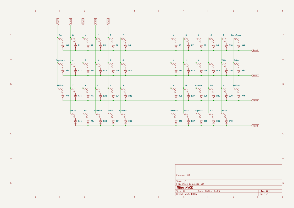
Esquema electrónico completo de cómo sería un teclado:
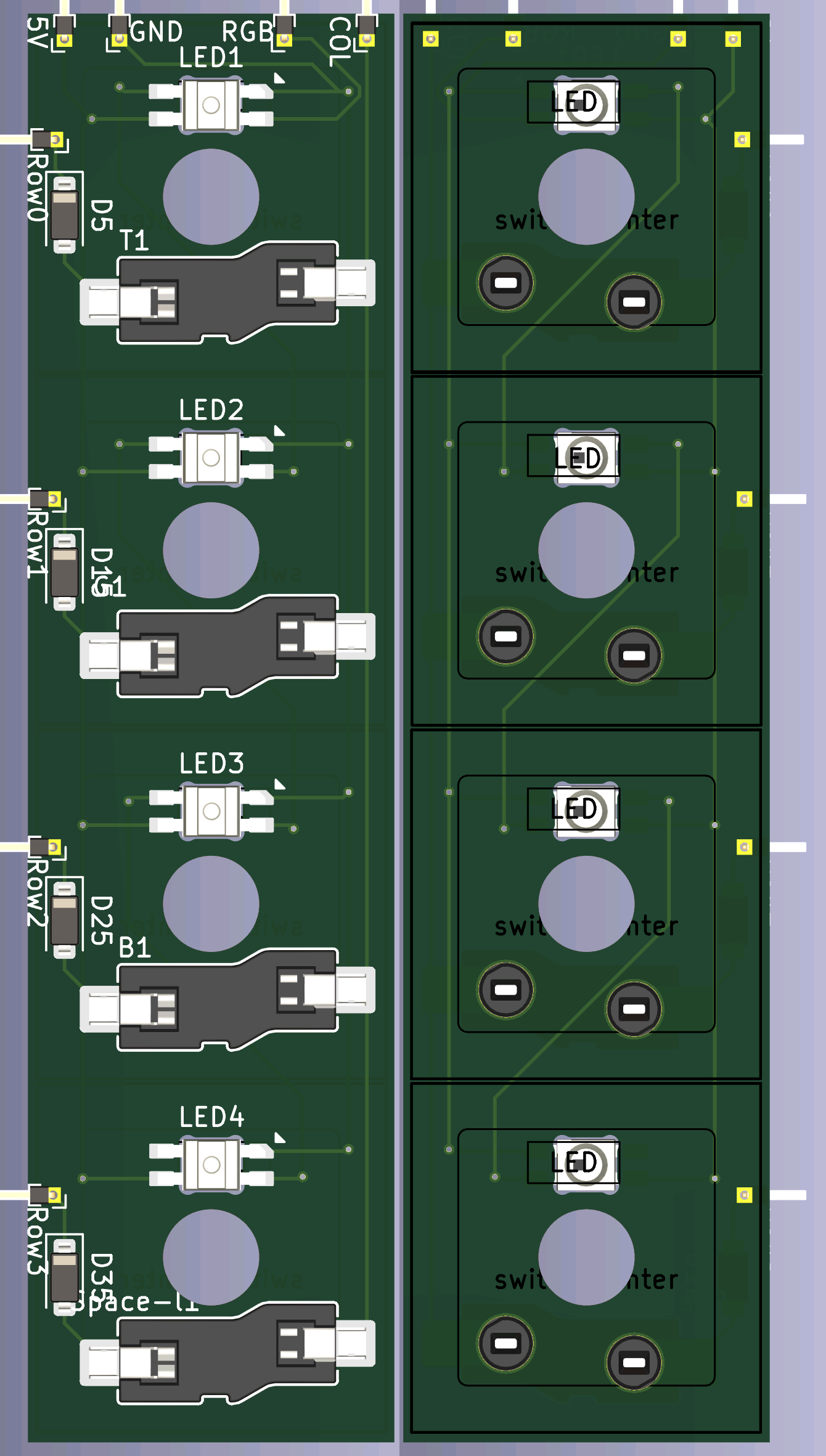
Esquema de la placa de pruebas:
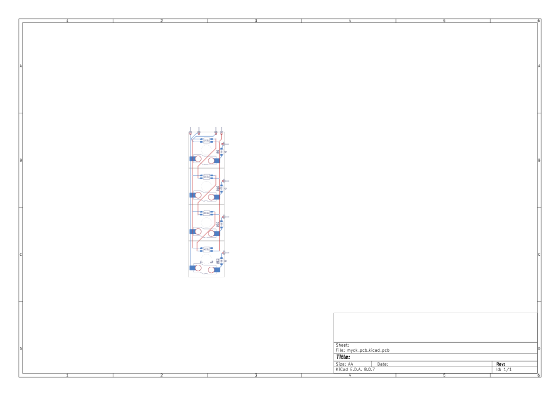
Sólo las pistas para la placa de pruebas:
| Qty | Value | Footprint | References |
|---|---|---|---|
| 8 | PinHeader_1x01_P1.00mm_Horizontal | Library:PinHeader_1x01_P1.00mm_Horizontal | 5V, COL, GND, RGB, Row0, Row1, Row2, Row3 |
| 4 | D | Library:D_SOD-123 | D5, D15, D25, D35 |
| 4 | MX_SK6812MINI-E | Library:LED_MX_6028R | LED1, LED2, LED3, LED4 |
| 4 | SW_Push_45deg | Library:SW_KS33_HS_KS-2P02B01-02_HS_1u | B1, G1, Space-l1, T1 |
It measures 20 × 78 mm and has 2 copper layers, 1.6 mm thick.
20 parts. The full list of its parts is on this page, with links to each part's symbol and footprint where PCBKit's library has them.
From the yuki/myck repository on GitHub, at the commit this page was made from: the board is myck_pcb/myck_pcb.kicad_pcb and its schematic myck_pcb/myck_pcb.kicad_sch. PCBKit opens the board in the browser, with nothing to install.
Its repository states no licence, so its author keeps all rights: ask yuki before reusing the design.


atopile/atopile
Design circuit boards with code! ✨ Get software-like design reuse 🚀, validation, version control and collaboration in hardware; starting with electronics ⚡️

davidphilipbarr/Sweep
Sweep - a small promicro based keyboard inspired by the Ferris.

rusefi/rusefi
rusefi - GPL internal combustion engine control unit

hoglet67/RGBtoHDMI
Bare-metal Raspberry Pi project that provides pixel-perfect sampling of Retro Computer RGB/YUV video and conversion to HDMI

hackclub/OnBoard
💡 Join 1,000 teenagers and make your first PCB with a $100 grant!

FreeYourStream/freedeck-hardware
all the stuff you need to build your own FreeDeck