4 layers52 × 39 mm
Motherboard
xjjak/LapCal
Building gloves that enable typing on a 34-key keyboard without an actual physical keyboard using IMUs and machine learning.
58 parts3

 yogesh8441/ESP32-S3-PCB-Design
A custom 2-layer ESP32-S3 development board designed in KiCad 10 featuring an onboard USB-to-UART interface, automatic boot/reset circuit, USB Type-C connectivity, onboard MPU6050 IMU sensor, and 3.3V regulated power…
My equation is an open-source printed circuit board by yogesh8441, from the yogesh8441/ESP32-S3-PCB-Design repository on GitHub. It is a 2-layer board of 41.7 × 47.8 mm with 29 parts on 74 nets, routed with 376 tracks and 41 vias.
It is built around the CH340C, ESP32-S3-WROOM-1-N8 and AP2112K-3.3, with the MPU-6050 and MMBT3904 among its other parts. Its parts include 10 resistors, 9 capacitors, 4 ICs, 2 diodes and 2 transistors. It belongs with the ESP32 boards of this library.


A custom 2-layer ESP32-S3 development board designed in KiCad 10 featuring an onboard USB-to-UART interface, automatic boot/reset circuit, USB Type-C connectivity, onboard MPU6050 IMU sensor, and 3.3V regulated power supply.
This project demonstrates the complete PCB design of an ESP32-S3 development board by integrating all essential hardware directly onto a custom PCB.
The design includes:
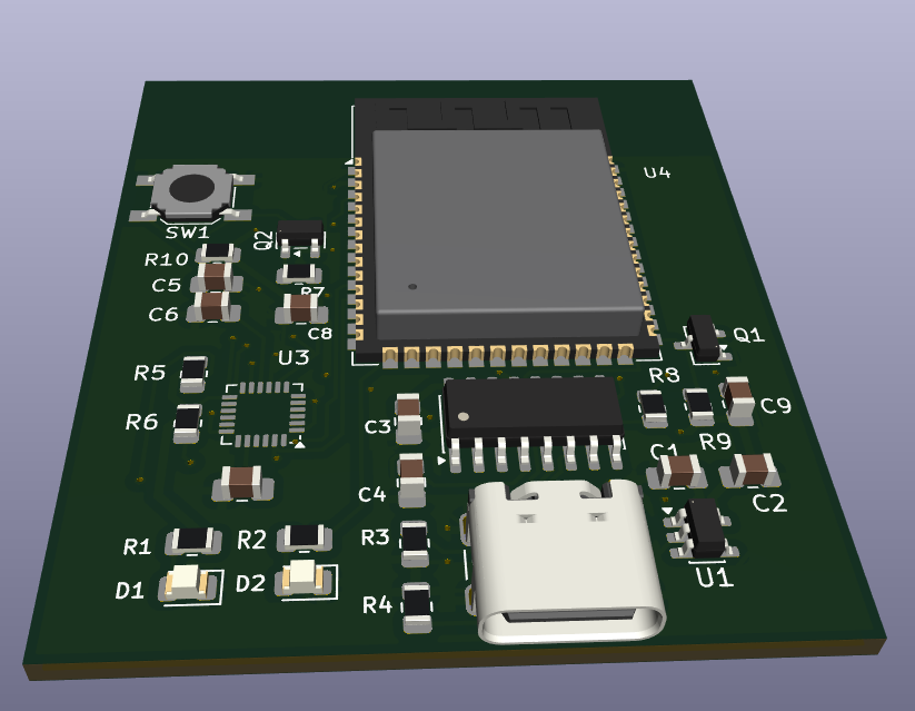
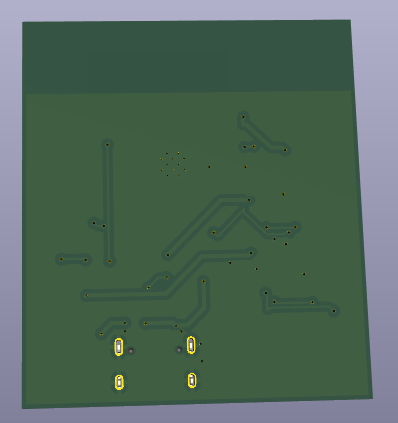
ESP32-S3-PCB/
│
├── Image/
│   ├── PCB_Top.png
│   ├── PCB_Bottom.png
│   └── Schematic.pdf
│
├── Gerber.zip
├── my equation.kicad_sch
├── my equation.kicad_pcb
├── my equation.kicad_pro
├── README.md| Component | Description |
|---|---|
| ESP32-S3-WROOM-1 | Main MCU |
| CH340C | USB to UART Converter |
| USB Type-C | Power & Programming |
| AP2112K | 3.3V LDO Regulator |
| MPU6050 | 6-Axis IMU Sensor |
| LEDs | Power & Status |
| Push Button | Reset |
Yogesh Kumar
| Qty | Value | Footprint | References |
|---|---|---|---|
| 4 | 100nF | Capacitor_SMD:C_0805_2012Metric_Pad1.18x1.45mm_HandSolder | C4, C5, C6, C8 |
| 4 | 10k | Resistor_SMD:R_0805_2012Metric | R7, R8, R9, R10 |
| 2 | 330 | Resistor_SMD:R_0805_2012Metric | R1, R2 |
| 2 | 4.7k | Resistor_SMD:R_0805_2012Metric | R5, R6 |
| 2 | 5.1k | Resistor_SMD:R_0805_2012Metric | R3, R4 |
| 2 | LED | LED_SMD:LED_0805_2012Metric | D1, D2 |
| 2 | MMBT3904 | Package_TO_SOT_SMD:SOT-23 | Q1, Q2 |
| 1 | 10nF | Capacitor_SMD:C_0805_2012Metric_Pad1.18x1.45mm_HandSolder | C7 |
| 1 | 10uF | Capacitor_SMD:C_0805_2012Metric_Pad1.18x1.45mm_HandSolder | C9 |
| 1 | 1uF | Capacitor_SMD:C_0805_2012Metric_Pad1.18x1.45mm_HandSolder | C1 |
| 1 | 2.2uF | Capacitor_SMD:C_0805_2012Metric_Pad1.18x1.45mm_HandSolder | C2 |
| 1 | AP2112K-3.3 | Package_TO_SOT_SMD:SOT-23-5 | U1 |
| 1 | C | Capacitor_SMD:C_0805_2012Metric_Pad1.18x1.45mm_HandSolder | C3 |
| 1 | CH340C | Package_SO:SOIC-16_3.9x9.9mm_P1.27mm | U2 |
| 1 | ESP32-S3-WROOM-1 | RF_Module:ESP32-S3-WROOM-1 | U4 |
| 1 | MPU-6050 | Sensor_Motion:InvenSense_QFN-24_4x4mm_P0.5mm | U3 |
| 1 | SW_Push | Button_Switch_SMD:SW_SPST_SKQG_WithoutStem | SW1 |
| 1 | USB_C_Receptacle_USB2.0_14P | Connector_USB:USB_C_Receptacle_GCT_USB4105-xx-A_16P_TopMnt_Horizontal | J1 |
xjjak/LapCal
Building gloves that enable typing on a 34-key keyboard without an actual physical keyboard using IMUs and machine learning.


angelowickramasinghe/Project-Drone
AeroFC-1S 1S brushed micro-quad flight controller (KiCad) — schematic, PCB, Gerbers, LCSC BOM

rmingon/nanro-uno
A compact and breadboard-friendly development board featuring the ATmega88PA microcontroller, onboard MPU-6050 6-axis IMU, USB-to-serial interface (CH340C), and ISP header.

gehadgad2019/Edge-Computing-Motion-PCB
A custom 2-layer edge-computing printed circuit board designed for motion sensing, localized signal processing, and low-latency I2C sensor communication.

mail2adnanyazik-bit/pandapute
A small, esp 32 based portable computer - an upgraded version of the cardputer adv, with more functionality, processing power, and ease of use.

It measures 41.7 × 47.8 mm and has 2 copper layers, 1.6 mm thick.
29 parts, built around the CH340C, ESP32-S3-WROOM-1-N8, AP2112K-3.3 and MPU-6050. The full list of its parts is on this page, with links to each part's symbol and footprint where PCBKit's library has them.
From the yogesh8441/ESP32-S3-PCB-Design repository on GitHub, at the commit this page was made from: the board is my equation.kicad_pcb and its schematic my equation.kicad_sch. PCBKit opens the board in the browser, with nothing to install.
Its repository states no licence, so its author keeps all rights: ask yogesh8441 before reusing the design.