

2 layers420.3 × 95.3 mm

 ymkn/henge402
A compact 40% keyboard with 12-column row staggered layout in 12.75u width.
Henge40 PCB is an open-source printed circuit board by ymkn, from the ymkn/henge40 repository on GitHub, published under the MIT licence. It is a 2-layer board of 245.3 × 78.6 mm with 93 parts on 64 nets, routed with 435 tracks and 48 vias.
It is built around the RP2040-TINY and 1N4148W. Its parts include 43 switches, 41 diodes and 1 IC. It belongs with the keyboards and input boards and the RP2040 boards of this library.
A compact 40% keyboard with 12-column row staggered layout in 12.75u width.
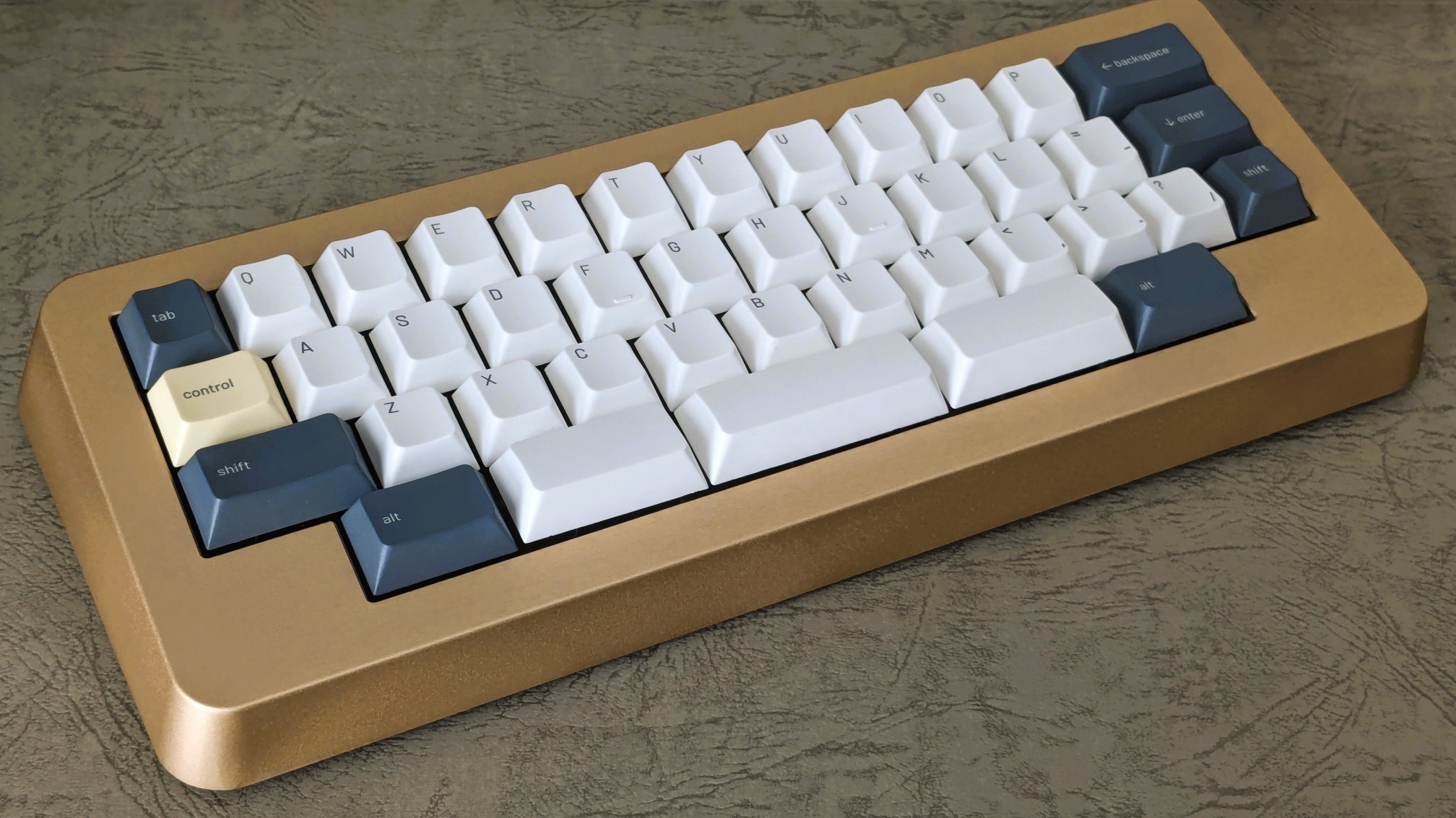
This keyboard was inspired by Menhir.
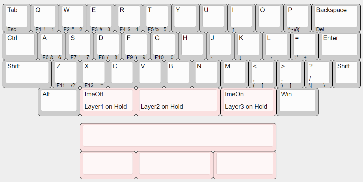
You can also customize the layout using Vial.
See Build Guide.
This project is licensed under the MIT License, see the LICENSE file for details.
However, this does not apply to logo data (image files, KiCAD footprints, etc.) included in the resources of this project. Please contact us for secondary use.
| Qty | Value | Footprint | References |
|---|---|---|---|
| 41 | 1N4148W | ymknlib_Various:D_SOD-123 | D1, D2, D10, D11, D12, D13, D14, D15, D16, D17, D18, D19, D20, D21, D22, D23 +25 |
| 37 | SW_Push | PCM_marbastlib-mx:SW_MX_HS_CPG151101S11_1u | SW1, SW10, SW11, SW12, SW13, SW14, SW15, SW16, SW17, SW18, SW19, SW20, SW21, SW21_1, SW22, SW23 +21 |
| 3 | SW_Push | PCM_marbastlib-mx:SW_MX_HS_CPG151101S11_1.5u | SW7, SW35, SW40 |
| 2 | SW_Push | PCM_marbastlib-mx:SW_MX_HS_CPG151101S11_1.75u | SW3, SW39 |
| 1 | henge40_logo:henge40_logotype | ||
| 1 | ymknlogo:1unekokey | ||
| 1 | SW_Push | PCM_marbastlib-mx:SW_MX_HS_CPG151101S11_1.25u | SW2 |
| 1 | rp2040-tiny | ymknlib_Waveshare_RP2040-Zero:Waveshare_RP2040-Zero_SMD | U1 |
The 87 most common of 93 parts.
It measures 245.3 × 78.6 mm and has 2 copper layers, 1.2 mm thick.
93 parts, built around the RP2040-TINY and 1N4148W. The full list of its parts is on this page, with links to each part's symbol and footprint where PCBKit's library has them.
From the ymkn/henge40 repository on GitHub, at the commit this page was made from: the board is KiCAD/PCB/Henge40_PCB.kicad_pcb and its schematic KiCAD/PCB/Henge40_PCB.kicad_sch. PCBKit opens the board in the browser, with nothing to install.
Its repository publishes it under the MIT licence: you may reuse it on that licence's terms (keep the author's notice, and for a copyleft licence share your changes alike).


partlyhuman/floopydrive
The Floopy Drive, an open-source flashcart for Casio Loopy


fossasia/pslab-hardware
PSLab Hardware Design and Schematics https://pslab.io