2 layers
Nrf bga
github-linguist/linguist
Language Savant. If your repository's language is being reported incorrectly, send us a pull request!
12 parts14kMIT

 Yhass131/kicad-learning
Working through KiCad from scratch — datasheet reading, custom symbols, custom footprints, and eventually full board layouts. Following Steppe School's tutorial playlist.
KiKad101 is an open-source printed circuit board by Yhass131, from the Yhass131/kicad-learning repository on GitHub. It is a 2-layer board of 17 × 20 mm with 12 parts on 9 nets, routed with 60 tracks and 8 vias.
Its parts include 4 diodes, 3 capacitors, 3 resistors and 1 IC.
Working through KiCad from scratch — datasheet reading, custom symbols, custom footprints, and full board layouts, from schematic capture through fabrication files. Following Steppe School's KiCad tutorial playlist.
This repo is a public log of my progress: every component library, footprint, and board I build while learning, along with notes on what each step actually taught me.
kicad-learning/
├── libraries/
│   ├── symbols/           # Custom .kicad_sym files
│   └── footprints/        # Custom .pretty footprint libraries
├── projects/
│   └── led-driver/        # Full board: schematic, PCB, fabrication files
│       └── fabrication/   # Gerbers + BOM submitted to PCBWay
├── datasheets/            # Reference datasheets for parts used
└── images/ # Screenshots used in this READMEPart: CAT4104VP2 — GT3 (LED driver)
Datasheet review. Pulled the pin assignments, absolute maximum ratings, and the recommended land pattern out of the datasheet.
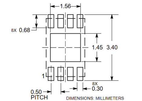
Footprint parameters:
820.50 mm0.30 mm0.68 mm2.72 mmRow spacing isn't given directly — it's the center-to-center distance between opposite pads, so I derived it from the overall land pattern width minus one pad length.
Symbol. Built the schematic symbol in the Symbol Editor with pin numbers, pin names, and electrical types set to match the datasheet.
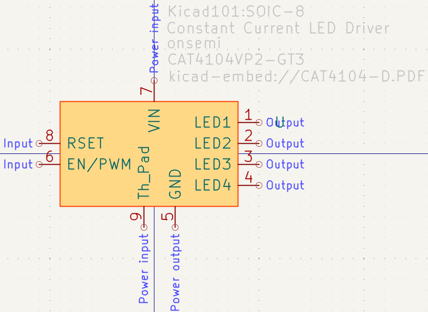
Schematic symbol for CAT4104VP2.
Footprint. Built the matching footprint in the Footprint Editor using the recommended land pattern — pads, silkscreen outline, courtyard, and pin 1 marker.
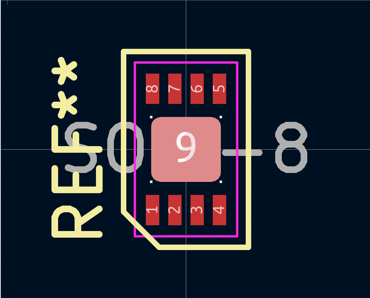
Footprint for CAT4104VP2 (GT3).
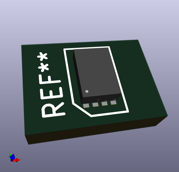
3D preview with the model assigned.
Part: 10164359-00011LF (USB connector)
This component acts as the board's power source.
Datasheet review.
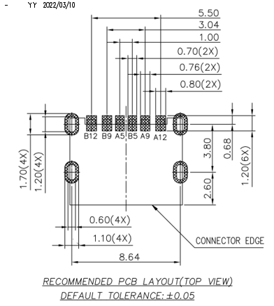
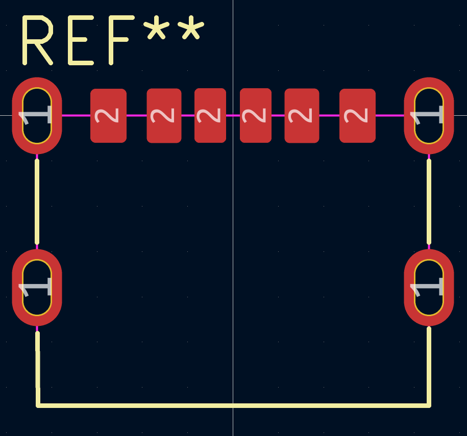
Similar approach to the LED driver for the square pads, but the oval pads are different — they're plated through-holes, used for parts that need a mechanical anchor through the board. In this case, the USB plug is secured to the board through those four holes.
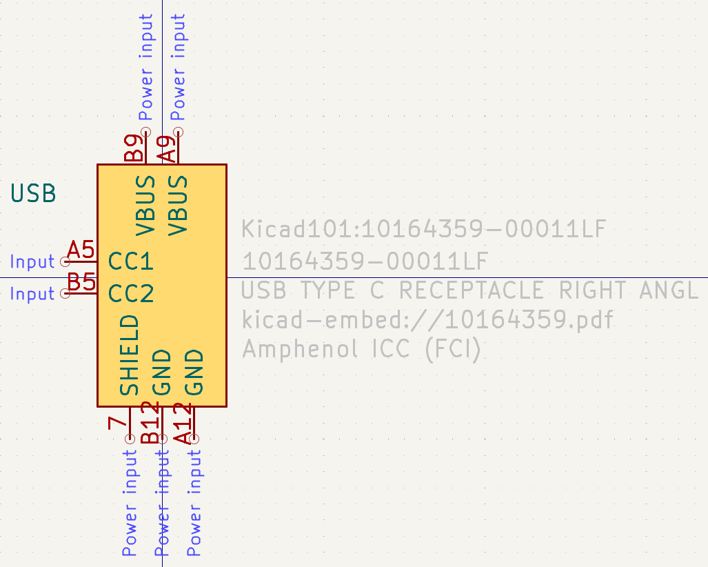
Symbol for USB connector 10164359-00011LF
Footprint.
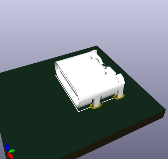
3D preview
Part: 158301265A (LED)
Datasheet review.
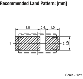
Same approach as before for the square pads.
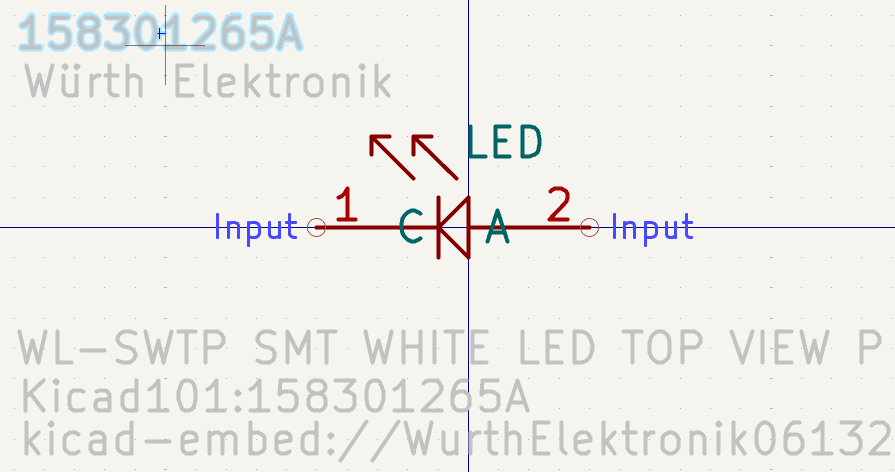
Symbol for LED 158301265A
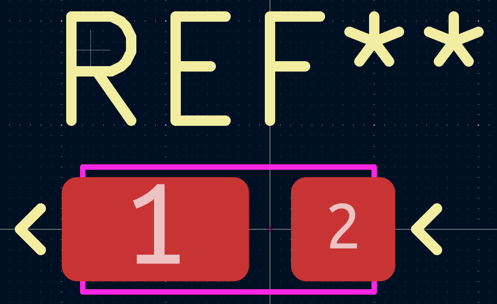
Footprint.
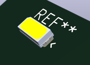
3D preview
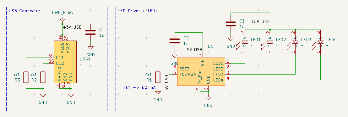
This schematic connects all the components to achieve a single goal: the LED driver keeps the LEDs lit, and both the driver and the LEDs are powered by the USB connector section. The +5V_USB tags are net labels — any tags sharing the same name are treated as electrically connected, removing the need for wires spanning across the schematic or between sections.
After finishing the design, the Electrical Rules Checker (ERC) was used to validate the schematic. Most issues found in this simple project were solved with minor adjustments in the Symbol Editor.
What I learned:
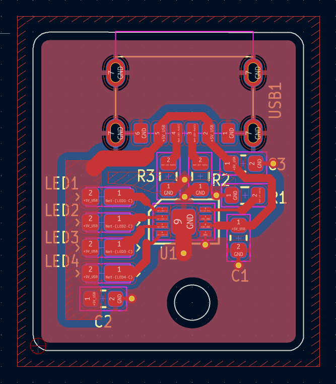
Top-level board footprint.
Before routing, set up the board's physical stackup in Board Setup — layer count, dielectric and copper layer thicknesses, and copper weight — so trace-width/impedance calculations and DRC behave correctly downstream. With the stackup defined, routed the traces, set trace widths, and added filled copper zones (ground/power pours) with proper net assignment, following best-practice pour clearance and stitching.
Ran the ERC again and traced each error and warning back to its source — sometimes in the top-level schematic, sometimes in an individual component's schematic symbol or footprint. Kept checking and fixing until everything cleared, then cleaned up the silkscreen.
To send the design out for fabrication with PCBWay, I needed the Gerber files and a bill of materials (BOM). Gerbers were straightforward to export from the PCB editor. The BOM took more work — I had to reformat it in the Schematic Editor to match PCBWay's expected format. Downloaded both into a manufacturing folder and uploaded them to PCBWay for review.
To use the custom libraries in your own KiCad project:
libraries/symbols/libraries/footprints/9.0Windows 11| Qty | Value | Footprint | References |
|---|---|---|---|
| 4 | ~ | Kicad101:158301265A | LED1, LED2, LED3, LED4 |
| 3 | 1u | Capacitor_SMD:C_0603_1608Metric | C1, C2, C3 |
| 2 | 5k1 | Resistor_SMD:R_0603_1608Metric | R2, R3 |
| 1 | 2k1 | Resistor_SMD:R_0603_1608Metric | R1 |
| 1 | ~ | Kicad101:10164359-00011LF | USB1 |
| 1 | ~ | Kicad101:SOIC-8 | U1 |
github-linguist/linguist
Language Savant. If your repository's language is being reported incorrectly, send us a pull request!


google/mozc-devices
Circuit diagrams and firmware source code for Gboard DIY keyboards


hackclub/OnBoard
💡 Join 1,000 teenagers and make your first PCB with a $100 grant!

VoronDesign/Voron-Tap
Tap is a nozzle-based z-probe for the V2 and Trident printer designs. The entire toolhead moves to trigger an optical switch. Tap offers many advantages:

stacksmashing/pico-tpmsniffer
A simple, very experimental TPM sniffer for LPC bus
It measures 17 × 20 mm and has 2 copper layers, 1.6 mm thick.
12 parts. The full list of its parts is on this page, with links to each part's symbol and footprint where PCBKit's library has them.
From the Yhass131/kicad-learning repository on GitHub, at the commit this page was made from: the board is projects/KiKad101.kicad_pcb and its schematic projects/KiKad101.kicad_sch. PCBKit opens the board in the browser, with nothing to install.
Its repository states no licence, so its author keeps all rights: ask Yhass131 before reusing the design.