4 layers75 × 71 mm

 YetAnotherElectronicsChannel/AES5067
An IP-Core for AES50 protocol
Aes50 trion is an open-source printed circuit board by YetAnotherElectronicsChannel, from the YetAnotherElectronicsChannel/AES50 repository on GitHub, published under the GPL-3.0 licence. It is a 4-layer board of 99 × 55 mm with 213 parts on 175 nets, routed with 2,030 tracks and 401 vias.
It is built around the T20Q100F3C4. Its parts include 112 resistors, 56 capacitors, 10 diodes, 8 ICs and 4 connectors. It belongs with the interfaces and adapters boards of this library.
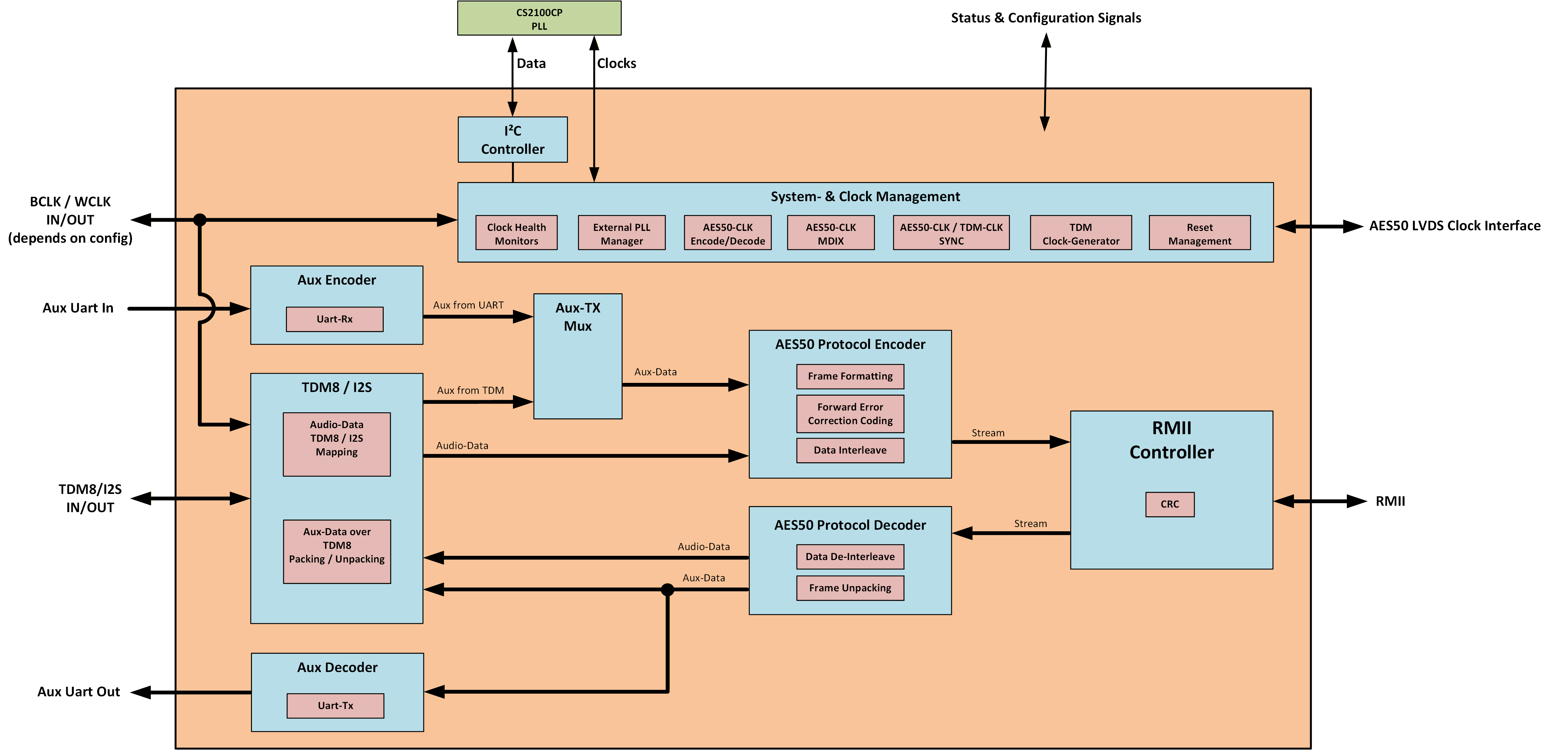
An implementation of the AES50 protocol in vanilla VHDL.
I started developing this IP around end of 2024 - originally with some other intention.
However I decided to make this project public with the purpose to be used in the fabulous OpenX32 project.
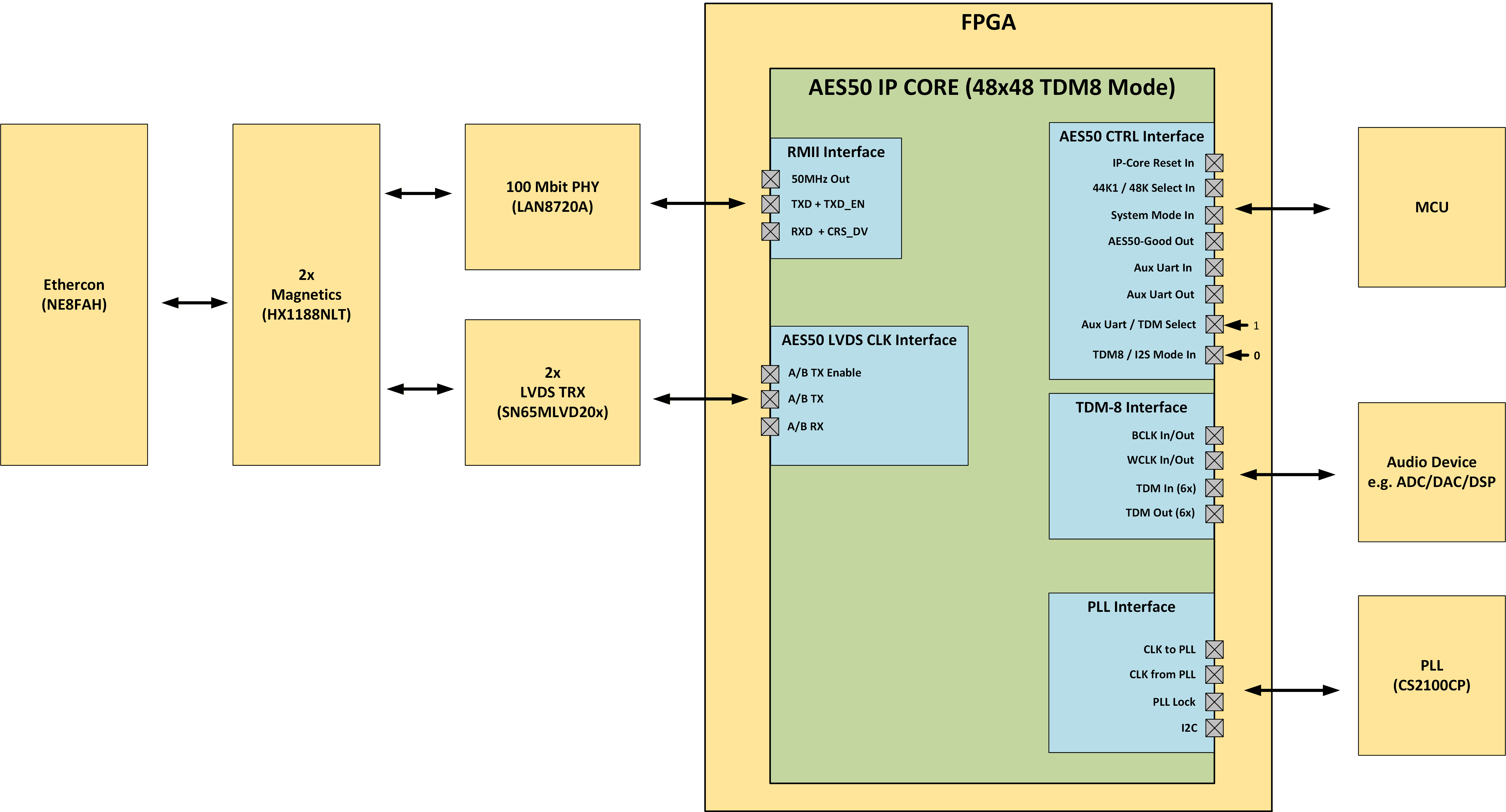
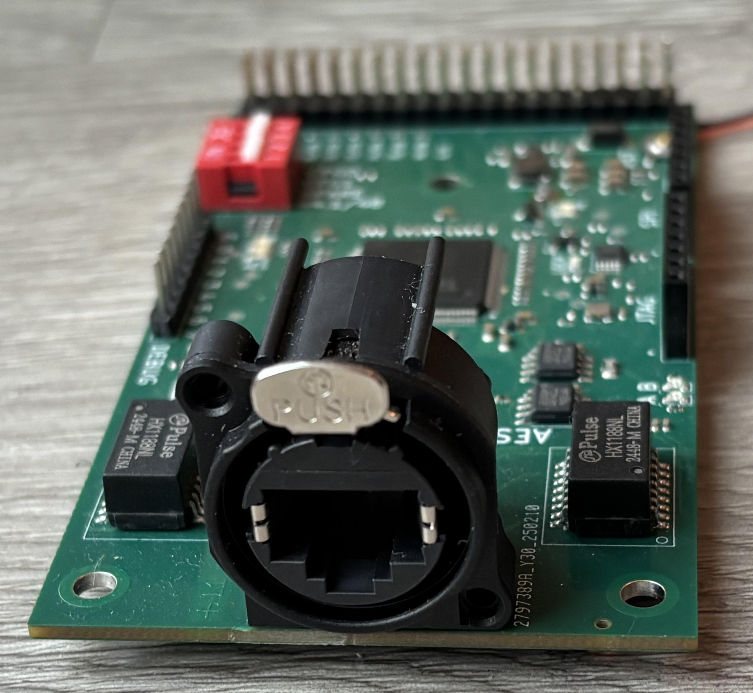
Therefore, this IP was developed fully independent/separated from the OpenX32 project and comes instead with a reference implementation on a custom PCB (also included in this repo) designed around an Efinix Trion T20 FPGA.
Integration into the OpenX32 project is still a to-do work.. But I'm sure those guys will manage :)
At the end of October 2026, I published a resource-optimized, functionally compatible version of this IP core, targeting the constrained FPGAs of the OpenX32 project: AES50v2
Before asking any detailed questions about functionality or implementation of this IP, please make sure you read and understood the public available AES50 specification which can be downloaded here.
Otherwise I might not answer to your request.
| Signal | Direction | Type | Description |
|---|---|---|---|
| clk50_i | in | std_logic | 50 MHz Clock for the Ethernet Logic |
| clk100_i | in | std_logic | 100 MHz Clock for the Core Logic |
| rst_i | in | std_logic | Synchronous Reset (100 MHz clock-domain) |
| fs_mode_i | in | std_logic_vector(1 downto 0) | Sample-Rate Select
|
| sys_mode_i | in | std_logic_vector(1 downto 0) | System-Mode Select
|
| tdm8_i2s_mode_i | in | std_logic | Interface Select
|
| aux_tx_tdm_uart_select_i | in | std_logic | Aux-Data-Mode
|
| rmii_crs_dv_i | in | std_logic | RMII Data Valid Receive from PHY |
| rmii_rxd_i | in | std_logic_vector(1 downto 0) | RMII Data from PHY |
| rmii_tx_en_o | out | std_logic | RMII Data Valid Transmit to PHY |
| rmii_txd_o | out | std_logic_vector(1 downto 0) | RMII Data to PHY |
| phy_rst_n_o | out | std_logic | PHY Reset (active low) |
| aes50_clk_a_rx_i | in | std_logic | AES50 Clock A Receive |
| aes50_clk_a_tx_o | out | std_logic | AES50 Clock A Transmit |
| aes50_clk_a_tx_en_o | out | std_logic | AES50 Clock A Enable LVDS Output Driver |
| aes50_clk_b_rx_i | in | std_logic | AES50 Clock B Receive |
| aes50_clk_b_tx_o | out | std_logic | AES50 Clock B Transmit |
| aes50_clk_b_tx_en_o | out | std_logic | AES50 Clock B Enable LVDS Output Driver |
| clk_1024xfs_from_pll_i | in | std_logic | Clock from external PLL (1024× fs) |
| pll_lock_n_i | in | std_logic | External PLL Lock Status (active low) |
| clk_to_pll_o | out | std_logic | Clock to external PLL |
| pll_mult_value_o | out | natural | External PLL multiplication-factor |
| pll_init_busy_i | in | std_logic | PLL init busy status |
| mclk_o | out | std_logic | Master Clock (256x fs) - derived (divided by x4) from PLL - independent of System-Mode Select |
| wclk_o | out | std_logic | Word Clock Output (if our IP is I2S/TDM Master) |
| bclk_o | out | std_logic | Bit Clock Output (if our IP is I2S/TDM Master) |
| wclk_readback_i | in | std_logic | Word Clock Readback (direct from FPGA-Pin - always needed) |
| bclk_readback_i | in | std_logic | Bit Clock Readback (direct from FPGA-Pin - always needed) |
| wclk_out_en_o | out | std_logic | Word Clock Output Enable (high if IP is I2S/TDM Master) |
| bclk_out_en_o | out | std_logic | Bit Clock Output Enable (high if IP is I2S/TDM Master) |
| tdm_i | in | std_logic_vector(6 downto 0) | 6x TDM8 Data Input + 1x TDM8 Aux Data Input (only needed in 48x48 mode) |
| tdm_o | out | std_logic_vector(6 downto 0) | 6x TDM8 Data Output + 1x TDM8 Aux Data Output (only needed in 48x48 mode) |
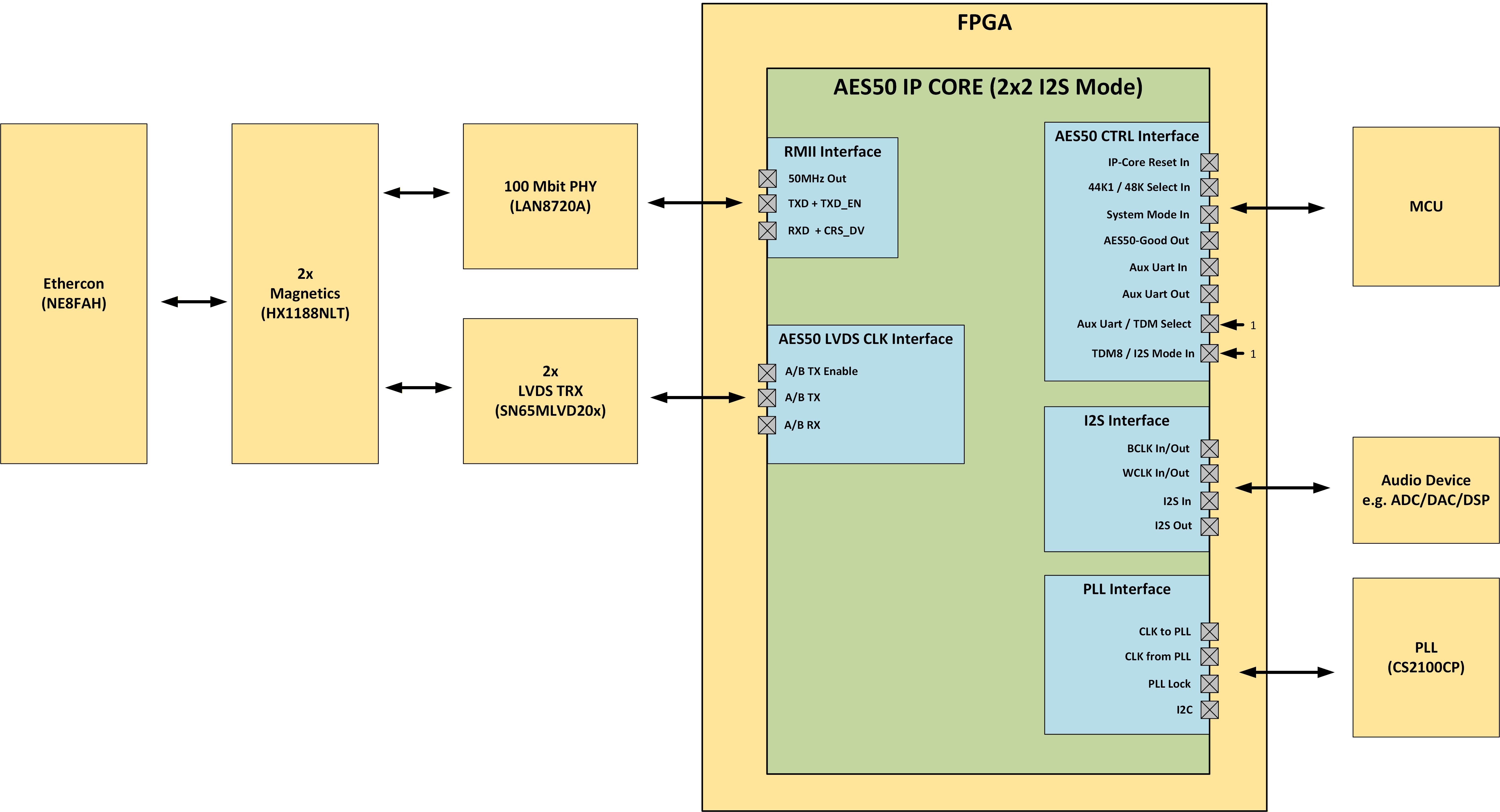
| i2s_i | in | std_logic | I2S Input (only needed in 2x2 mode) |
| i2s_o | out | std_logic | I2S Output (only needed in 2x2 mode) |
| aes_ok_o | out | std_logic | AES50 Link Status (high when connection established) |
| dbg_o | out | std_logic_vector(7 downto 0) | Various internal debug signals |
| uart_o | out | std_logic | UART output (received data from the AES50 AUX tunnel) |
| uart_i | in | std_logic | UART input (data to send over AES50 AUX-tunnel) |
AES50 provides (as part of the protocol) an auxiliary data channel with a fixed bandwidth of roughly 5 Mbit/s (the exact rate depends on the selected sample rate, as the auxiliary data stream is synchronous with the audio transmission).
According to the AES50 specification, there was a proposal (though not mandatory) to use standard Ethernet frames that could be tunneled through this auxiliary data channel - (ever wondered about the mysterious Ethernet port on the DN9630?) -> Therefore I assume that this proposed approach using virtual Ethernet frames is also used in other AES50 devices on the market.
However, additional mechanisms are required to transmit Ethernet frames through the auxiliary channel - specifically bit-stuffing and data-scrambling.
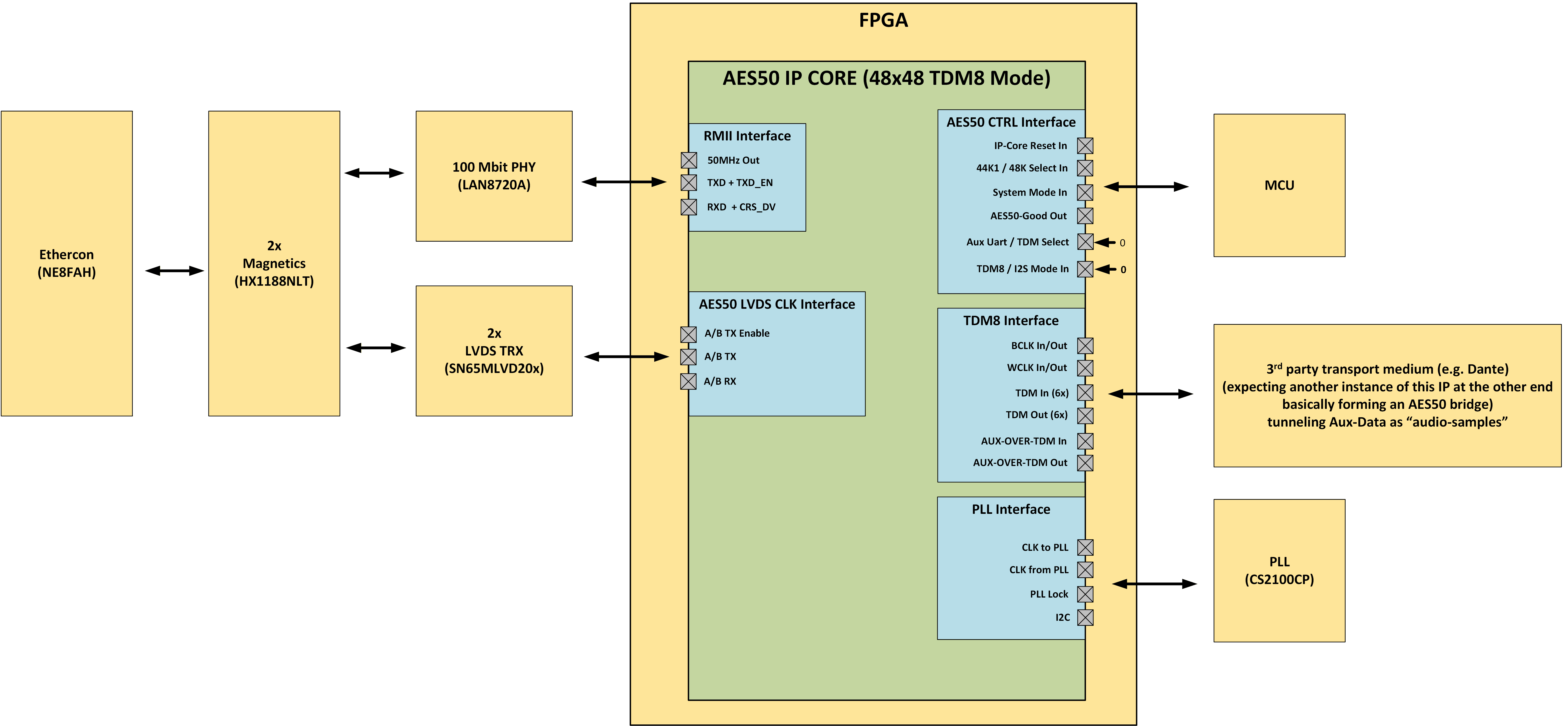
Since the bitstream is synchronous with the audio transmission, this IP enables sending and receiving the aux-bitstream over the TDM8 interface.
Internally, the IP handles the bitstream as 16-bit words, and the TDM module distributes the auxiliary data evenly across the eight TDM slots as 24-bit “samples.”
The extra 8 bits act as an overlay protocol to ensure correct interpretation of the auxiliary words when tunneling them over a 3rd party audio-transportation-medium.
If the TDM-Aux-RX/TX pins of two instances of this IP are cross-connected, it allows transparent tunneling of the auxiliary data channel as long as synchronicity and bit-consistency is ensured.
A similar concept appears to be implemented in the Appsys Multiverter, which tunnels AES50 auxiliary data as eight audio channels through a Dante network to maintain head-amp remote control.
It is also possible to send and receive data over the aux-data-tunnel with a UART connection.
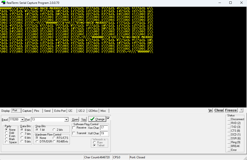
See here an example print-out of a Wing-Rack connected.
A small Arduino example shows how to self-identify and remotely control the head amps (gain & phantom power) of AES50 devices.
This example uses a Raspberry Pi Pico (RP2040), which acts as a command bridge between a computer and the UART terminal connected to the FPGA/AES50 IP core.
The device identifies itself as an X32 Full-Size and the head amps can be controlled via a serial terminal using the following command examples:
gain:ch1@20 → Sets gain on channel 1 to +20 dBphantom:ch5@1 → Enables +48V on channel 5phantom:ch5@0 → Disables +48V on channel 5The gain-ranges may be interpreted differently with different devices. You will find some info in the comments of the code-example.
This example is currently configured for controlling a Wing. Make sure that Remote-HA-Control over AES50 is enabled in the console settings.
See more information here: Unofficial Protocol Description
Special thanks to Christian Nöding for reverse-engineering the proprietary protocol and Thomas Zint (Behringer R&D) for helping with the checksum calculation.
Note: The transmission of channel-names does not work yet.
Warning: When this IP is in I2S/TDM slave-mode (sys_mode_i = "10"), make ultimately sure, that BCLK/WCLK is stable before releasing the IP's reset.
AES50 protocol has a pulse-width modulation mechanism in the outgoing (LVDS-)clock signals which needs to be synchronized to the incoming I2S/TDM clock.
This is only done once after reset. You must ensure externally, if WCLK/BCLK has changed or was unstable, this IP core runs again through a new reset.
In I2S mode, BCLK is 64*fs : 32-Bit per Slot (24-Bit Audio + 8 Bit Padding).
3.072 MHz for 48k mode and 2.8224 MHz for 44k1. No other I2S configuration is supported besides this.
This is valid for all system-modes.
BCLK is supposed to be 12.288 MHz for 48k or 11.2896 MHz for 44k1 : 32-Bit per Slot (24-Bit Audio + 8 Bit Padding).
No other TDM configuration is supported besides this.
This is valid for all system-modes.
When the IP is TDM master, the WCLK will be high for 8 BCLK cycles.

WCLK must be only high for one BCLK pulse (but can be longer of course)

In I2S mode, only I0/O0 will be used as in+out.
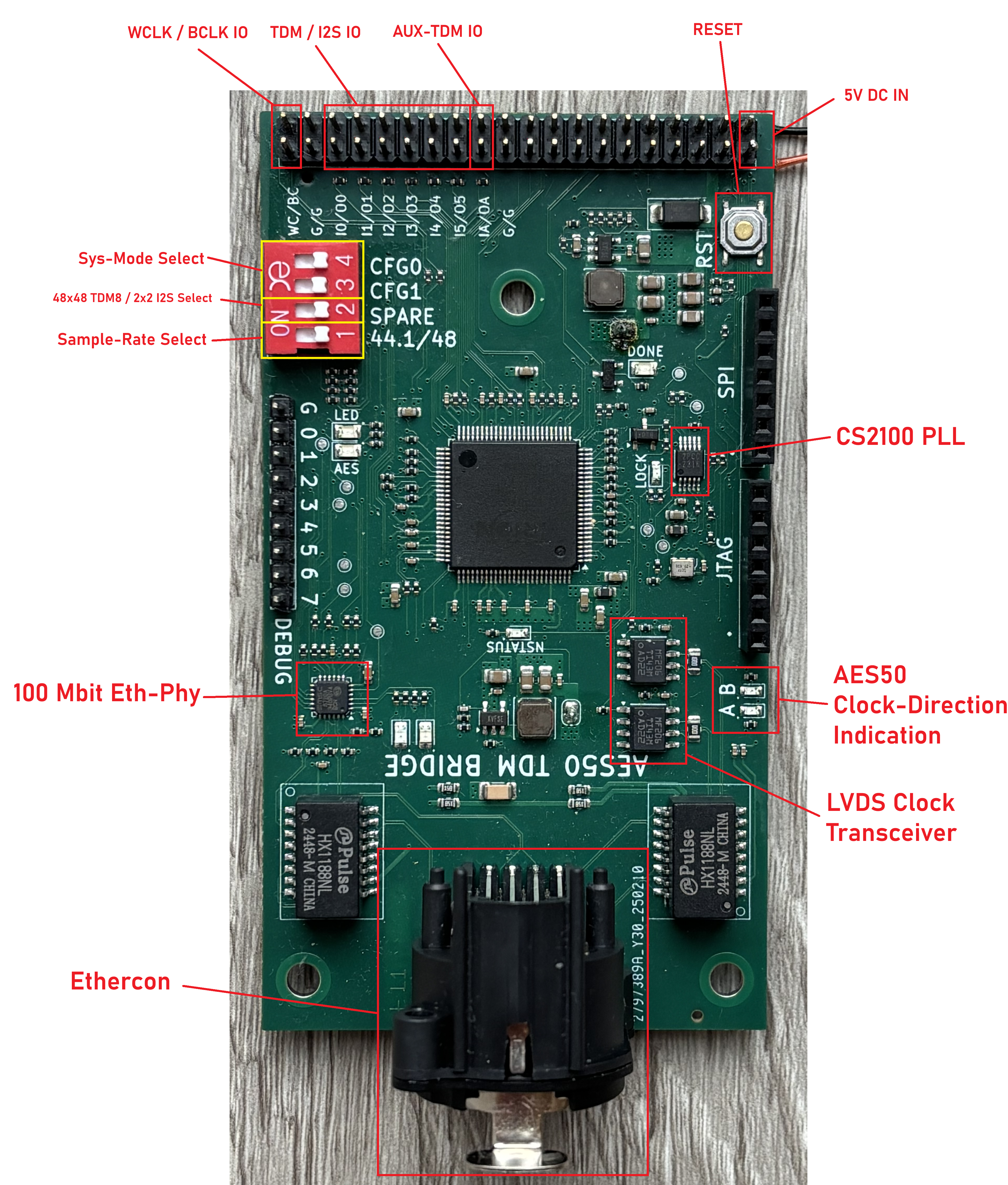
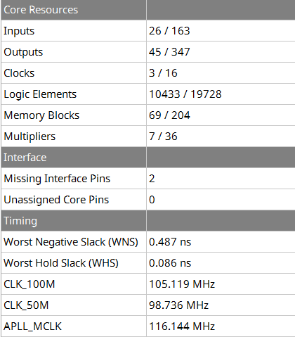
This is the resource utilization for a full configuration (all sample-rates and operation modes supported, dual TDM/I2S support, PLL-I2C driver etc.).
Resource utilization depends on actual used configuration.
Especially if core is configured for e.g. I2S only operation, the utilization is reduced drastically (the TDM-Serdes is still a rather resource-inefficient implementation as of today).
Reference FPGA: Efinix Trion T20Q100F3 (Speedgrade: 4) using Efinity 2025.1.110.5.9 toolchain.

The Startup Sequencing must be timed very precisely.
The Ethernet frame containing the "2048x ASSM-marker" in the header must be tightly aligned with the modulated-clock-pulses on the LVDS signaling.
This happens in 48k as follows: The IP waits until the clock-pulse-modulation happens. (It is assumed it will happen again after 2048x WCLK). When the clock-pulse-modulation happened, a timer starts with the duration of approx. 2042x (2048-6) WCLK timeframes.
Then the TDM-serializer starts recording samples into the FIFO to the AES50-TX-module.
The AES50-TX-Module waits until 6 samples (basically 288 samples as it is 6 samples * 48 channels) are in the FIFO.
The first ethernet-frame transmitted after this startup-sequence will contain the ASSM-marker in the frame-header and will be aligned with the 2048x modulated clock-pulse.
This also explains the mysterious "first_transmit_counter" values on the top-level files.
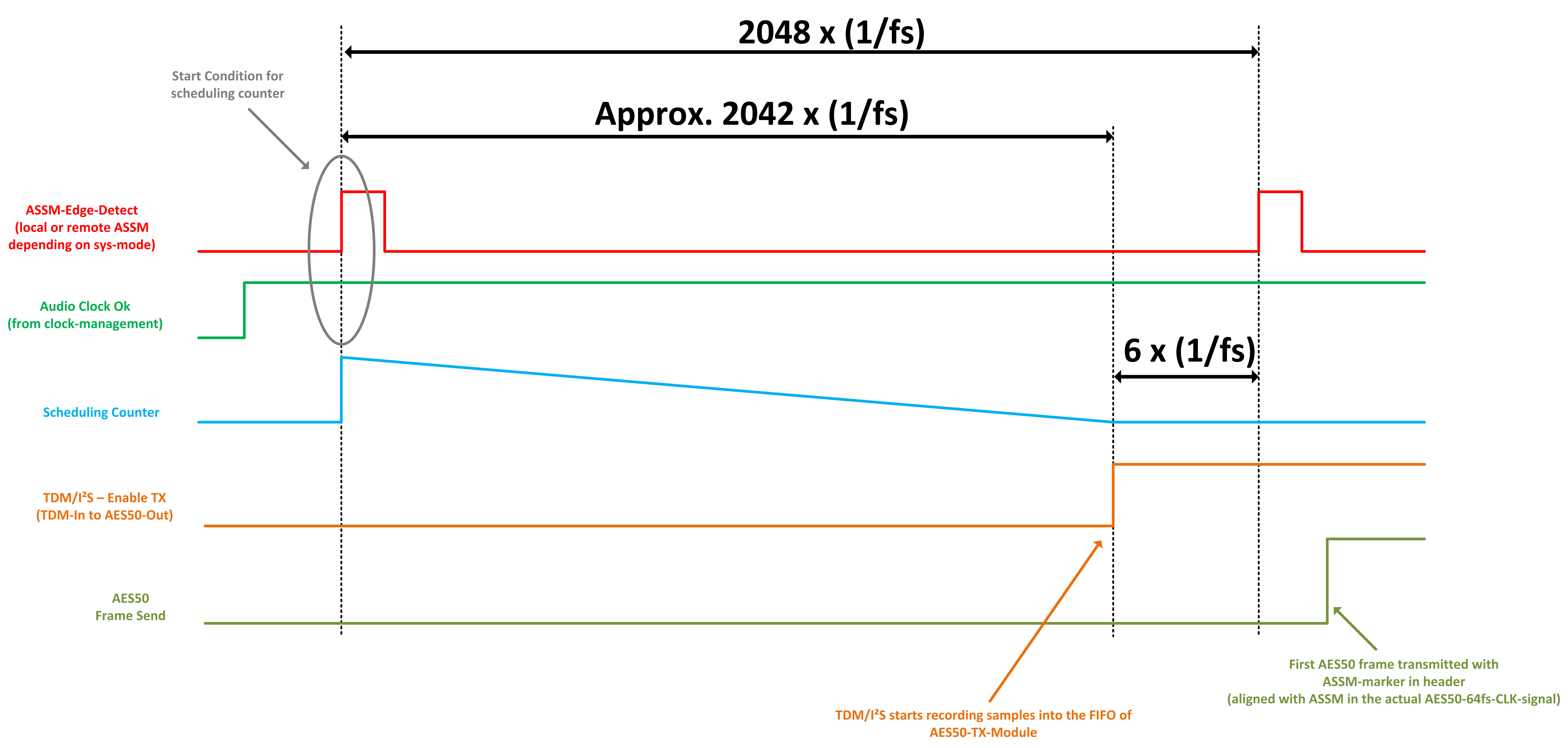
In 44k1 the same mechanism applies, but with a duration of 2048-11 = 2037 WCLK cycles wait time.
I also attached now the testbenches I used.
Please see the testbenches as WIP as I modified them as needed and those testbenches might not work out of the box. So this is more of a "playground" rather than a professional verification testbench.
Copyright (c) 2025 Markus Noll (YetAnotherElectronicsChannel)
This IP core is free software: you can redistribute it and/or modify it under the terms of the GNU General Public License as published by the Free Software Foundation, either version 3 of the License, or (at your option) any later version.
This IP core is distributed in the hope that it will be useful, but WITHOUT ANY WARRANTY; without even the implied warranty of MERCHANTABILITY or FITNESS FOR A PARTICULAR PURPOSE. See the GNU General Public License for more details.
You should have received a copy of the GNU General Public License along with this IP core. If not, see https://www.gnu.org/licenses/.
Any other use — including use in other projects or commercial applications — is not permitted without a separate written license agreement.
Third-party components included in this repository may be licensed under different terms (for example, GPLv3). These components retain their original licenses and are clearly marked in the source header.
| Qty | Value | Footprint | References |
|---|---|---|---|
| 50 | 10k/0402 | Resistor_SMD:R_0402_1005Metric | R13, R14, R15, R16, R18, R20, R100, R101, R102, R103, R104, R106, R108, R110, R111, R112 +34 |
| 35 | 100n/16V/0402 | Capacitor_SMD:C_0402_1005Metric | C1, C2, C10, C11, C12, C13, C14, C15, C18, C19, C20, C21, C22, C23, C24, C26 +19 |
| 18 | 100/0402 | Resistor_SMD:R_0402_1005Metric | R47, R52, R53, R54, R55, R56, R57, R58, R60, R62, R63, R64, R65, R66, R67, R68 +2 |
| 16 | 33/0402 | Resistor_SMD:R_0402_1005Metric | R5, R6, R7, R8, R24, R29, R48, R59, R61, R70, R71, R72, R73, R83, R84, R86 |
| 10 | 1k/0402 | Resistor_SMD:R_0402_1005Metric | R12, R19, R27, R28, R46, R49, R50, R81, R105, R109 |
| 10 | TestPoint | TestPoint:TestPoint_Pad_D1.0mm | TP1, TP2, TP3, TP4, TP5, TP6, TP7, TP8, TP9, TP10 |
| 9 | 22u/25V/0805 | Capacitor_SMD:C_0805_2012Metric | C40, C43, C44, C47, C50, C51, C54, C55, C56 |
| 8 | 1u/50V/0603 | Capacitor_SMD:C_0603_1608Metric | C4, C16, C17, C25, C29, C32, C36, C46 |
| 4 | 49.9/0402 | Resistor_SMD:R_0402_1005Metric | R1, R2, R3, R4 |
| 4 | 75/0603 | Resistor_SMD:R_0603_1608Metric | R10, R11, R22, R23 |
| 4 | LED 0603 Red (C2286) | LED_SMD:LED_0603_1608Metric | D3, D4, D5, D8 |
| 4 | LED 0805 Green (C2297) | LED_SMD:LED_0805_2012Metric | D1, D6, D7, D10 |
| 2 | 100/0805 | Resistor_SMD:R_0805_2012Metric | R25, R30 |
| 2 | 100k/0402 | Resistor_SMD:R_0402_1005Metric | R90, R107 |
| 2 | 12k/0402 | Resistor_SMD:R_0402_1005Metric | R17, R74 |
| 2 | 22k/0402 | Resistor_SMD:R_0402_1005Metric | R87, R88 |
| 2 | 22p/50V/0402 | Capacitor_SMD:C_0402_1005Metric | C42, C49 |
| 2 | 4k7/0402 | Resistor_SMD:R_0402_1005Metric | R79, R80 |
| 2 | 600Ω/0603 (C1002) | Inductor_SMD:L_0603_1608Metric | FB1, FB2 |
| 2 | FH2.54-09-07PZD (C7500776) | MarkusFootprintLibrary:FH2.54-09-07PZD | J2, J4 |
| 2 | FHD4020S-2R2MT (C602029) | Inductor_SMD:L_APV_ANR4020 | L1, L2 |
| 2 | HX1188NLT (C9363) | MarkusFootprintLibrary:HX1188NL | TR1, TR2 |
| 2 | SN65MLVD206DR (C2671006) | Package_SO:SOIC-8_3.9x4.9mm_P1.27mm | U2, U3 |
| 2 | SY8089AAAC (C78988) | Package_TO_SOT_SMD:SOT-23-5 | U7, U8 |
| 2 | SolderJumper_2_Open | Jumper:SolderJumper-2_P1.3mm_Open_RoundedPad1.0x1.5mm | JP1, JP2 |
| 1 | 10u/10V/0603 | Capacitor_SMD:C_0603_1608Metric | C37 |
| 1 | 1n/2kV/1206 | Capacitor_SMD:C_1206_3216Metric | C6 |
| 1 | 25MHz (C7431317) | Oscillator:Oscillator_SMD_ECS_2520MV-xxx-xx-4Pin_2.5x2.0mm | X2 |
| 1 | CS2100CP-CZZR (C2663267) | Package_SO:MSOP-10_3x3mm_P0.5mm | U6 |
| 1 | DSWB04LHGET (C99418) | MarkusFootprintLibrary:DSWB04LHGET | SW2 |
| 1 | LAN8720A (C45223) | Package_DFN_QFN:VQFN-24-1EP_4x4mm_P0.5mm_EP2.5x2.5mm_ThermalVias | U1 |
| 1 | LED 0805 Yellow (C2296) | LED_SMD:LED_0805_2012Metric | D2 |
| 1 | MMBT5551 (C2145) | Package_TO_SOT_SMD:SOT-23 | Q1 |
| 1 | Neutrik NE8FAH (C368497) | MarkusFootprintLibrary:Neutrik NE8FAH | X1 |
| 1 | PZ254-2-20-Z-2.5-G1 (C18198015) | Connector_PinHeader_2.54mm:PinHeader_2x20_P2.54mm_Vertical | J1 |
| 1 | SS34 40V 3A (C8678) | Diode_SMD:D_SMA | D9 |
| 1 | Standard Header 2.54mm | Connector_PinHeader_2.54mm:PinHeader_1x09_P2.54mm_Vertical | J3 |
| 1 | T20Q100F3C4 | Package_QFP:LQFP-100_14x14mm_P0.5mm | U4 |
| 1 | TLV803SDBZR (C132016) | Package_TO_SOT_SMD:SOT-23 | U5 |
| 1 | TS-1187A-B-A-B (C318884) | MarkusFootprintLibrary:TS-1187A-B-A-B | SW1 |
It measures 99 × 55 mm and has 4 copper layers, 1.6 mm thick.
213 parts, built around the T20Q100F3C4. The full list of its parts is on this page, with links to each part's symbol and footprint where PCBKit's library has them.
From the YetAnotherElectronicsChannel/AES50 repository on GitHub, at the commit this page was made from: the board is Hardware Design/KiCad Files/aes50_trion.kicad_pcb and its schematic Hardware Design/KiCad Files/AES50_FrontEnd.kicad_sch. PCBKit opens the board in the browser, with nothing to install.
Its repository publishes it under the GPL-3.0 licence: you may reuse it on that licence's terms (keep the author's notice, and for a copyleft licence share your changes alike).


tuankoko567/LattePanda-MU-carrier-Board
Designing high-speed carrier board using KiCad, applying differential pair routing and length matching, studying impedance control and PCB stack-up planning, learning signal integrity and EMI-aware layout techniques.

AnasSarkiz/smart-nema14-motor-controller
STEPPERONLINE 14HM11-0404S controller — unrouted work-in-progress prototype; mechanical and electrical qualification pending


Nicolboy/KICAD-C2000-powershield
Shield d'isolation, alimentation et interconnexion pour TMS320 C2000, conçu sous KiCad 10.
