2 layers40 × 20 mm

 xtarke/iot_zephyr_samples3
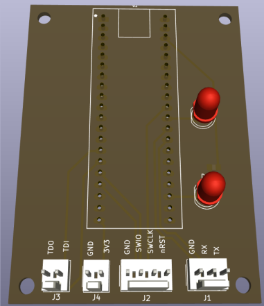
This documentation describes the hardware schematic for configuring an STM32 BlackPill as a Black Magic Probe (BMP) debugger.
Rp pico bmp probe is an open-source printed circuit board by xtarke, from the xtarke/iot_zephyr_samples repository on GitHub. It is a 2-layer board of 51.5 × 67.7 mm with 13 parts on 38 nets, routed with 50 tracks and 0 vias.
Its parts include 4 connectors, 2 resistors, 2 diodes and 1 IC. It belongs with the sensors and measurement and interfaces and adapters boards and the RP2040 boards of this library.
This documentation describes the hardware schematic for configuring an STM32 BlackPill as a Black Magic Probe (BMP) debugger. This design breaks out the essential debug and serial interfaces necessary for flashing and interacting with embedded targets.
The schematic details the pin routing from the BlackPill's microcontroller to dedicated external connectors, providing a unified interface for hardware debugging.
The following critical signals are exposed for target interaction:
SWDIO and SWCLK.TDI and TDO.TX and RX lines for target serial communication.RST), +3.3V, and GND.The design organizes these signals into specific pin headers for modular target connections:
+3.3V, GND) and other localized signal pairs.The schematic includes visual indicators to monitor the probe's state during execution:
PC14, typically used for general error or operational status indication
.
| Qty | Value | Footprint | References |
|---|---|---|---|
| 2 | Conn_01x02_Pin | Connector_Molex:Molex_KK-254_AE-6410-02A_1x02_P2.54mm_Vertical | J3, J4 |
| 2 | LED | LED_THT:LED_D5.0mm | D1, D2 |
| 2 | R | Resistor_SMD:R_0805_2012Metric_Pad1.20x1.40mm_HandSolder | R1, R2 |
| 1 | Conn_01x03_Pin | Connector_Molex:Molex_KK-254_AE-6410-03A_1x03_P2.54mm_Vertical | J1 |
| 1 | Conn_01x04_Pin | Connector_Molex:Molex_KK-254_AE-6410-04A_1x04_P2.54mm_Vertical | J2 |
| 1 | ~ | pill:Z_module_black_pill_STM32F411 | U1 |
The 9 most common of 13 parts.


samyk/magspoof
A portable device that can spoof/emulate any magnetic stripe, credit card or hotel card "wirelessly", even on standard magstripe (non-NFC/RFID) readers.

fossasia/pslab-scripts
Pocket Science Lab - Scripts for Sensor Experiments


willem-pennings/balancing-cube
A cube that balances itself in a corner or edge using reaction wheels

VoronDesign/Voron-Hardware
Cool Hardware designed by the Voron Design group

hoglet67/RGBtoHDMI
Bare-metal Raspberry Pi project that provides pixel-perfect sampling of Retro Computer RGB/YUV video and conversion to HDMI
It measures 51.5 × 67.7 mm and has 2 copper layers, 1.6 mm thick.
13 parts. The full list of its parts is on this page, with links to each part's symbol and footprint where PCBKit's library has them.
From the xtarke/iot_zephyr_samples repository on GitHub, at the commit this page was made from: the board is _debugger/black_magic_probe/rp_pico_bmp_probe.kicad_pcb and its schematic _debugger/black_magic_probe/rp_pico_bmp_probe.kicad_sch. PCBKit opens the board in the browser, with nothing to install.
Its repository states no licence, so its author keeps all rights: ask xtarke before reusing the design.