2 layers
Nrf bga
github-linguist/linguist
Language Savant. If your repository's language is being reported incorrectly, send us a pull request!
12 parts14kMIT

 wrongbaud/RPi_Hat_Template
KiCad template for a Raspberry Pi B+ Hat PCB.
RPi Hat is an open-source printed circuit board by wrongbaud, from the wrongbaud/RPi_Hat_Template repository on GitHub, published under the MIT licence. It is a 2-layer board of 65 × 56.5 mm with 12 parts on 54 nets, routed with 74 tracks and 0 vias.
% RPi B+ Hat
This is a project template for a Raspberry Pi B+ Hat.
This base project includes a PCB edge defined according to this specification. Both a thru-hole and a surface mount connector are provided, along with a different PCB edge for each. Just keep the PCB edge and connector type that you're using for your design and delete the others.
The component footprints used in this template are here.
The board outline looks like this:
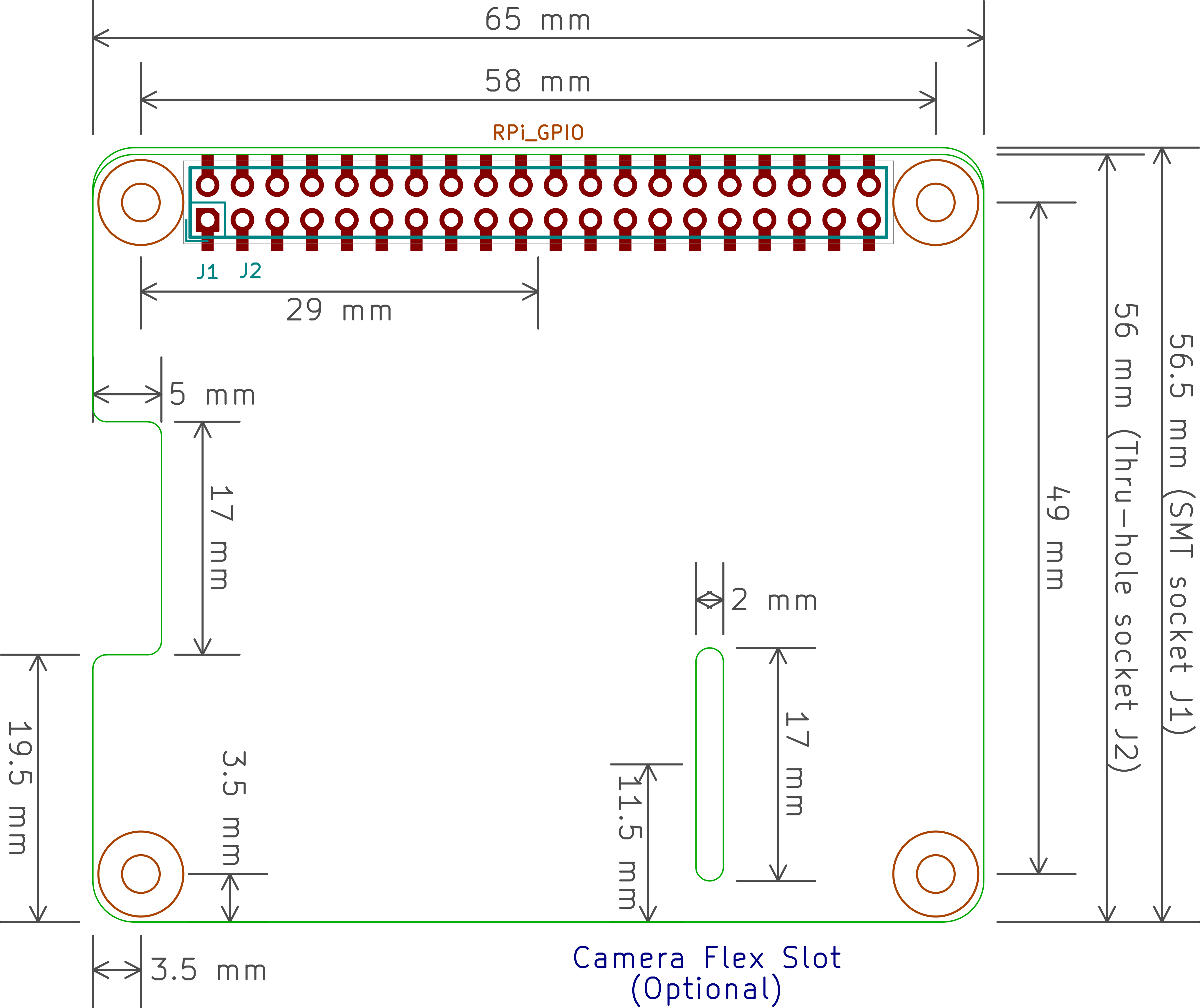
To use the Raspberry Pi Hat template with the through-hole connector, do the following:
To use the Raspberry Pi Hat template with the SMD connector, do the following:
(c)2015-2021 Dave Vandenbout.
| Qty | Value | Footprint | References |
|---|---|---|---|
| 4 | RPi_Hat:RPi_Hat_Mounting_Hole | , , , | |
| 1 | Conn_01x08_Female | Connector_PinHeader_2.54mm:PinHeader_1x08_P2.54mm_Vertical | J1 |
| 1 | Logic Analyzer Connector | Connector_PinHeader_2.54mm:PinHeader_1x08_P2.54mm_Vertical | J7 |
| 1 | Logic Level Selector | Connector_PinHeader_2.54mm:PinHeader_1x02_P2.54mm_Vertical | J4 |
| 1 | Logic Level Shifter - Target Side | Connector_PinHeader_2.54mm:PinHeader_1x10_P2.54mm_Vertical | J3 |
| 1 | Logic Level Shifter Pi Side | Connector_PinHeader_2.54mm:PinHeader_1x10_P2.54mm_Vertical | J5 |
| 1 | Output Enable | Connector_PinHeader_2.54mm:PinHeader_1x02_P2.54mm_Vertical | J6 |
| 1 | RPi_GPIO | RPi_Hat:Pin_Header_Straight_2x20 | J2 |
| 1 | USB_C_Plug_USB2.0 | Connector_USB:USB_C_Receptacle_GCT_USB4085 | P1 |
It measures 65 × 56.5 mm and has 2 copper layers, 1.6 mm thick.
12 parts. The full list of its parts is on this page, with links to each part's symbol and footprint where PCBKit's library has them.
From the wrongbaud/RPi_Hat_Template repository on GitHub, at the commit this page was made from: the board is RPi_Hat.kicad_pcb. PCBKit opens the board in the browser, with nothing to install.
Its repository publishes it under the MIT licence: you may reuse it on that licence's terms (keep the author's notice, and for a copyleft licence share your changes alike).
github-linguist/linguist
Language Savant. If your repository's language is being reported incorrectly, send us a pull request!


google/mozc-devices
Circuit diagrams and firmware source code for Gboard DIY keyboards


hackclub/OnBoard
💡 Join 1,000 teenagers and make your first PCB with a $100 grant!

VoronDesign/Voron-Tap
Tap is a nozzle-based z-probe for the V2 and Trident printer designs. The entire toolhead moves to trigger an optical switch. Tap offers many advantages:

stacksmashing/pico-tpmsniffer
A simple, very experimental TPM sniffer for LPC bus