4 layers26.7 × 21.9 mm
Buck Converter
murexrobotics/electrical
Highly integrated electronics design and printed circuit boards (PCBs) for the MATE ROV Competition. Attempt the impossible.
21 parts192MIT
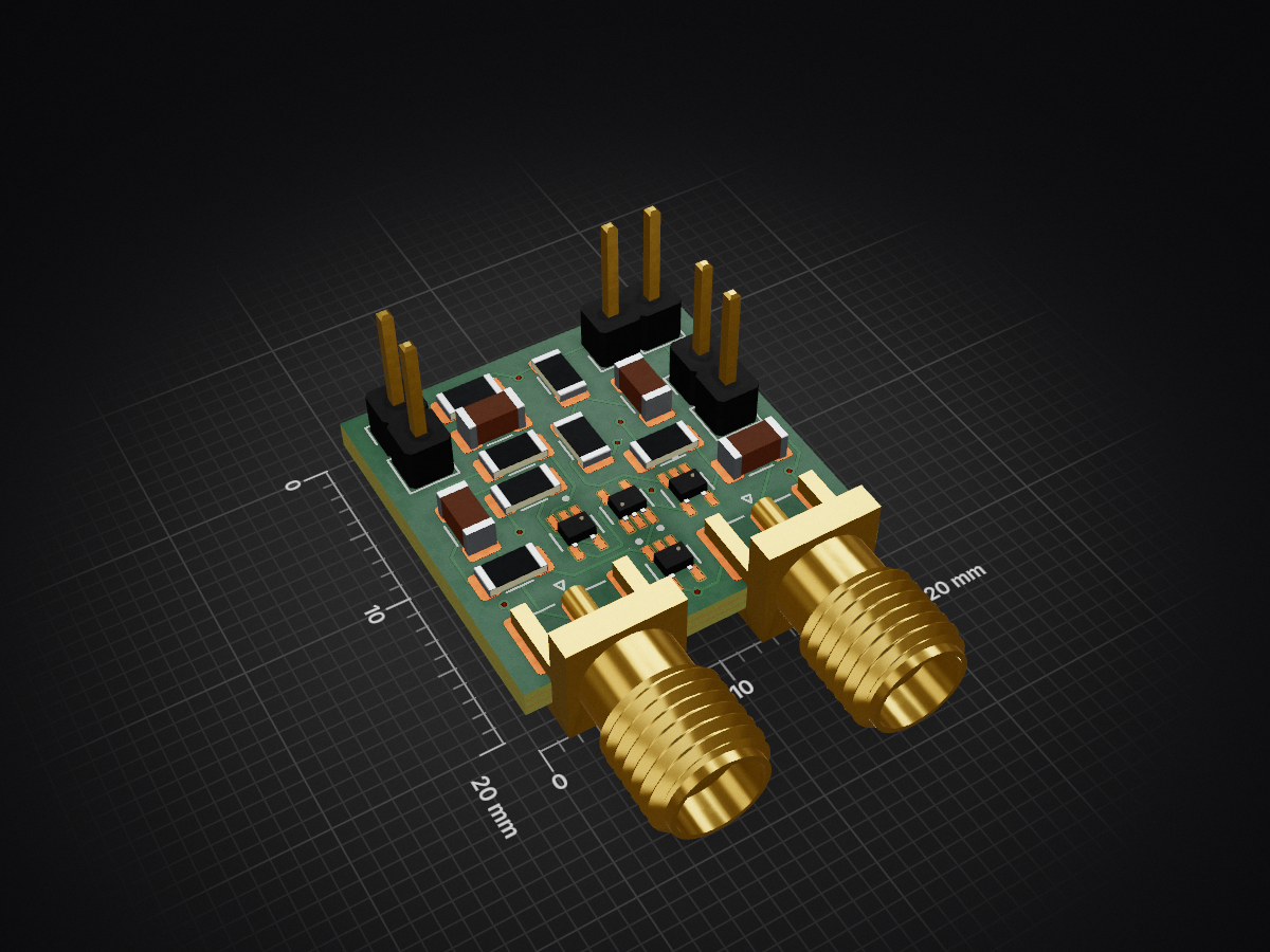
 Will946/Diff-Pair-Amplifier
A fully differential JFET-based amplifier designed to condition small analog signals from pressure transducers. The amplifier takes in a weak differential signal and amplifies it for readback by a microcontroller.
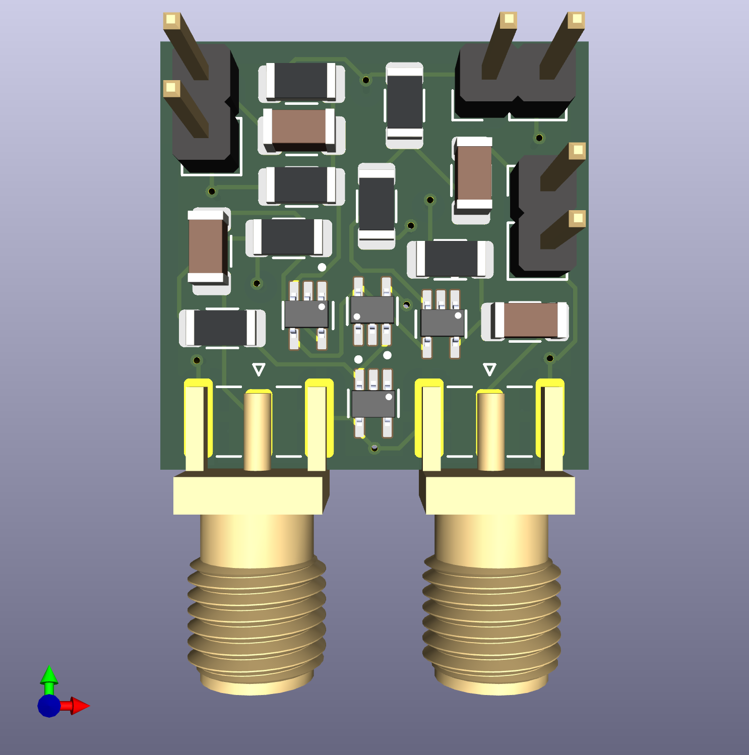
AMP PCB is an open-source printed circuit board by Will946, from the Will946/Diff-Pair-Amplifier repository on GitHub, published under the MIT licence. It is a 4-layer board of 20 × 20 mm with 21 parts on 20 nets, routed with 99 tracks and 10 vias.
It belongs with the audio and music boards of this library.
A fully differential JFET-based amplifier designed to condition small analog signals from pressure transducers. The amplifier takes in a weak differential signal and amplifies it for readback by a microcontroller. The design is compact enough to mount close to the sensor, minimizing noise pickup before amplification.
Typical use cases for this amplifier topology include:
The amplifier is a common-source differential pair using two JFE150DCKR N-channel JFETs with resistive drain loads, biased by a JFET current mirror tail current source.
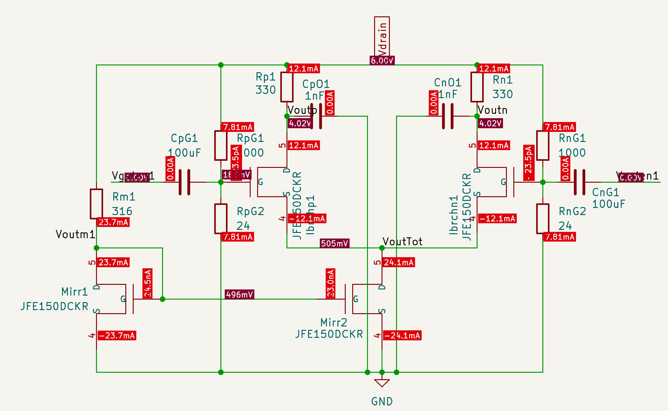
| Parameter | Value |
|---|---|
| Supply voltage (V_DD) | 8 V |
| Drain voltage (Voutp / Voutn) | 4.02 V |
| Drain current per branch | 12.1 mA |
| Tail current | 24.1 mA |
| Gate bias voltage | 188 mV |
| Total DC current | ~48 mA |
| Total DC power | ~0.38 W |
The drain voltage sits at 4.02 V - midway in the 0-8 V supply range - providing symmetric output swing headroom for both positive and negative signal excursions.
| Parameter | Simulated |
|---|---|
| Midband gain (Avd) | 20.5 dB |
| -3 dB frequency | 5.05 MHz |
| Unity gain frequency (UGF) | 51.6 MHz |
| Output Vpp (transient) | 1.09 V |
| Total DC current | ~48 mA |
| Power consumption | ~0.38 W |
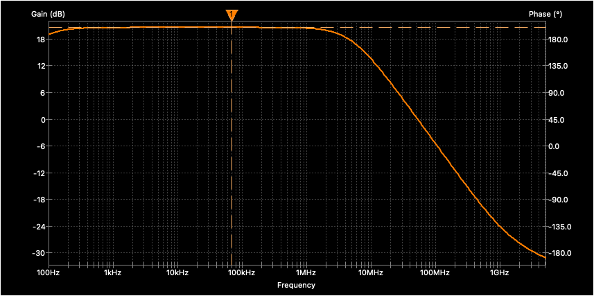
Simulated midband differential gain is 20.5 dB. In application this means the amplifier produces roughly 10x voltage amplification of the sensor signal before it reaches the microcontroller, giving the ADC a much larger and cleaner signal to digitize than the raw transducer output.
The -3 dB frequency is 5.05 MHz and the UGF is 51.6 MHz.
The -3 dB frequency is the point at which gain drops 3 dB from its midband value. Signals below this frequency are amplified at full gain; signals above it begin to attenuate. For a pressure transducer reading force on a robotic arm, relevant signal frequencies are well below 1 MHz, so the 5.05 MHz -3 dB comfortably covers the application bandwidth with margin to spare.
The UGF is the frequency at which gain falls to 0 dB - the amplifier is no longer amplifying above this point. At 51.6 MHz this sets the upper bound of useful operation and also indicates the stability behavior when used in a closed-loop system.
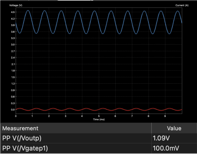
A 100 mVpp input sine wave at 1 kHz produces a clean 1.09 V peak-to-peak output with no visible clipping, confirming the amplifier operates linearly at this signal level and delivers sufficient swing to drive a microcontroller ADC input.
All simulations were run in ngspice via KiCAD.
DC Operating Point (.op)
AC Analysis
.ac dec 100 100 5GV(/Voutp) - V(/Voutn) in dBTransient Analysis
.tran 1u 10m| File | Description |
|---|---|
Differential_Pair_Amplifier.kicad_sch | Main schematic |
Differential_Pair_Amplifier.kicad_pcb | PCB layout |
Bodeplot.png | AC gain and phase vs frequency |
DC_Analysis.png | DC operating point simulation |
Transient_Analsyis.png | Transient input/output waveforms |
PCB.png | 3D render of PCB |
| Qty | Value | Footprint | References |
|---|---|---|---|
| 4 | JFE150DCKR | 348Footprint:TRANS_JFE150DCKR | Ibrchn1, Ibrchp1, Mirr1, Mirr2 |
| 3 | Conn_01x02_Pin | Connector_PinHeader_2.54mm:PinHeader_1x02_P2.54mm_Vertical | PHD1, PHGN1, PHGP1 |
| 2 | 1000 | Resistor_SMD:R_1206_3216Metric | RnG1, RpG1 |
| 2 | 100uF | Capacitor_SMD:C_1206_3216Metric | CnG1, CpG1 |
| 2 | 1nF | Capacitor_SMD:C_1206_3216Metric | CnO1, CpO1 |
| 2 | 24 | Resistor_SMD:R_1206_3216Metric | RnG2, RpG2 |
| 2 | 330 | Resistor_SMD:R_1206_3216Metric | Rn1, Rp1 |
| 2 | Conn_Coaxial | Connector_Coaxial:SMA_Samtec_SMA-J-P-H-ST-EM1_EdgeMount | VnO1, VpO1 |
| 1 | 316 | Resistor_SMD:R_1206_3216Metric | Rm1 |
| 1 | LOGO | 348Footprint:Untitled | G*** |
It measures 20 × 20 mm and has 4 copper layers, 1.6 mm thick.
21 parts. The full list of its parts is on this page, with links to each part's symbol and footprint where PCBKit's library has them.
From the Will946/Diff-Pair-Amplifier repository on GitHub, at the commit this page was made from: the board is PCB_Files/AMP_PCB.kicad_pcb and its schematic PCB_Files/AMP_PCB.kicad_sch. PCBKit opens the board in the browser, with nothing to install.
Its repository publishes it under the MIT licence: you may reuse it on that licence's terms (keep the author's notice, and for a copyleft licence share your changes alike).
murexrobotics/electrical
Highly integrated electronics design and printed circuit boards (PCBs) for the MATE ROV Competition. Attempt the impossible.

i2cjak/Framework_Expansion_Cards
In which i2cjak creates a new expansion card design every day until he is given a NICE Framework laptop

reneklootwijk/mideahvac-dongle
This repository contains the hardware design of a WiFi dongle for Midea-like airconditioners and humidifiers. Midea provides a WiFi dongle (SK102/SK103), either as optional feature or built-in, to control the appliances…


OpenSiPM/sipm-bias-control
Single channel silicon photomultipliers for high-speed fluorescence imaging

