6 layers105.6 × 100.9 mm

 whatnick/ctvt-pmod
CT and VT analog acquisition PMOD for Tiny Tapeout energy-monitor testing
Ctvt pmod is an open-source printed circuit board by whatnick, from the whatnick/ctvt-pmod repository on GitHub. It is a 2-layer board of 30 × 70 mm with 39 parts on 23 nets, routed with 287 tracks and 11 vias.
It is built around the PJ-002BH-SMT-TR, SJ-3523-SMT-TR and SMBJ18CA, with the SMF3.3CA among its other parts. Its parts include 13 resistors, 7 capacitors, 4 connectors, 2 diodes and 1 IC.


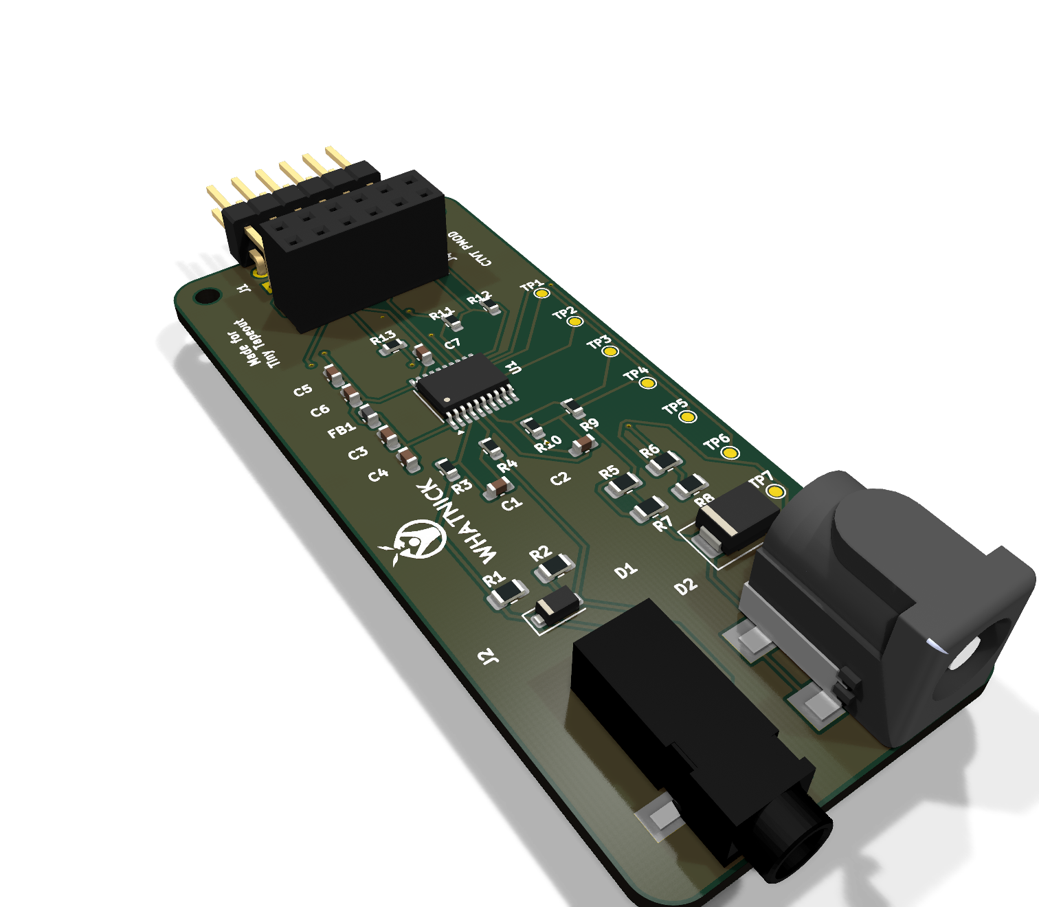
CTVT PMOD is a compact, open-hardware analog front end for phase-coherent current and voltage sampling. It uses a TI ADS131M02 dual 24-bit delta-sigma ADC and is intended for energy-monitoring DSP experiments, including Tiny Tapeout ASIC projects.
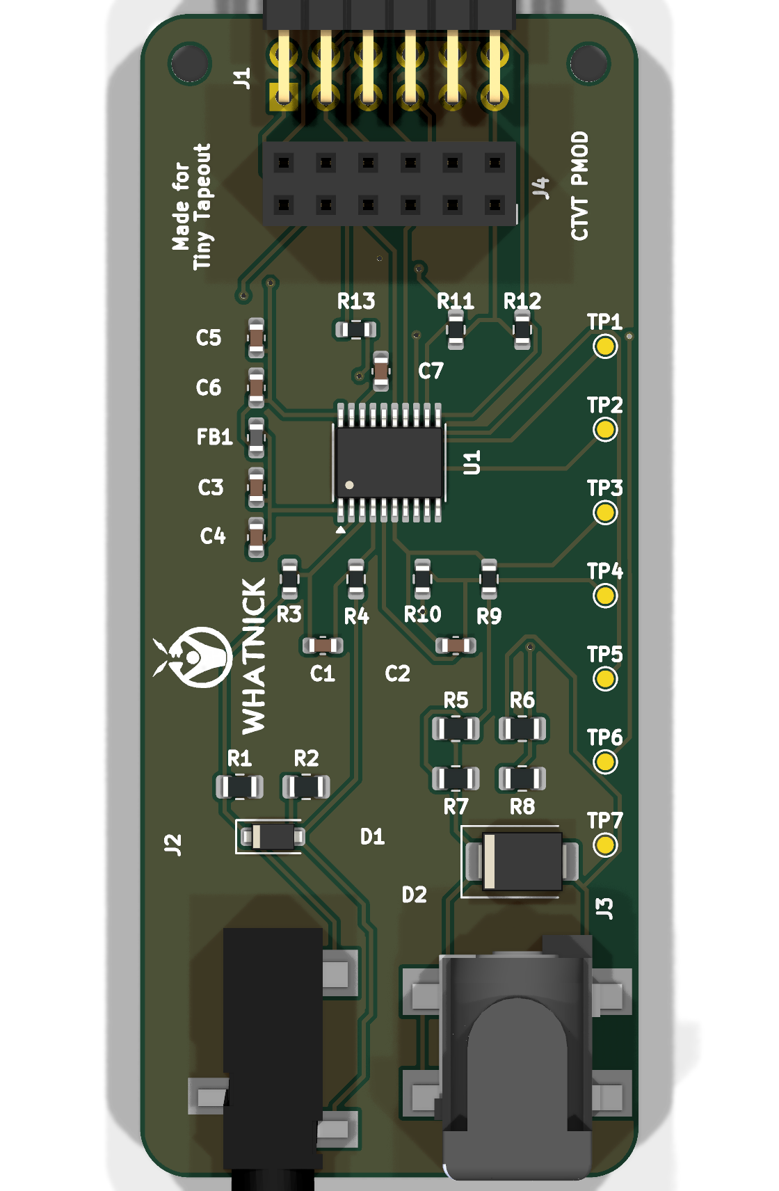
The routed KiCad 10 design is 30 mm x 70 mm with 3 mm corner radii and two 2.2 mm non-plated M2 mounting holes at the PMOD end. The PMOD connectors are centered together on one short edge; the CT and AC/AC transformer inputs face away from them at the opposite edge so adjacent PMODs remain usable. All routed signals use 0.25 mm traces with 0.20 mm copper clearance.
The narrow layout keeps the measurement front end beside other PMODs rather than blocking them. Both field connectors project beyond the board edge for comfortable cable access, while the vertical female header provides a second PMOD connection for stacking or logic-analyzer access.
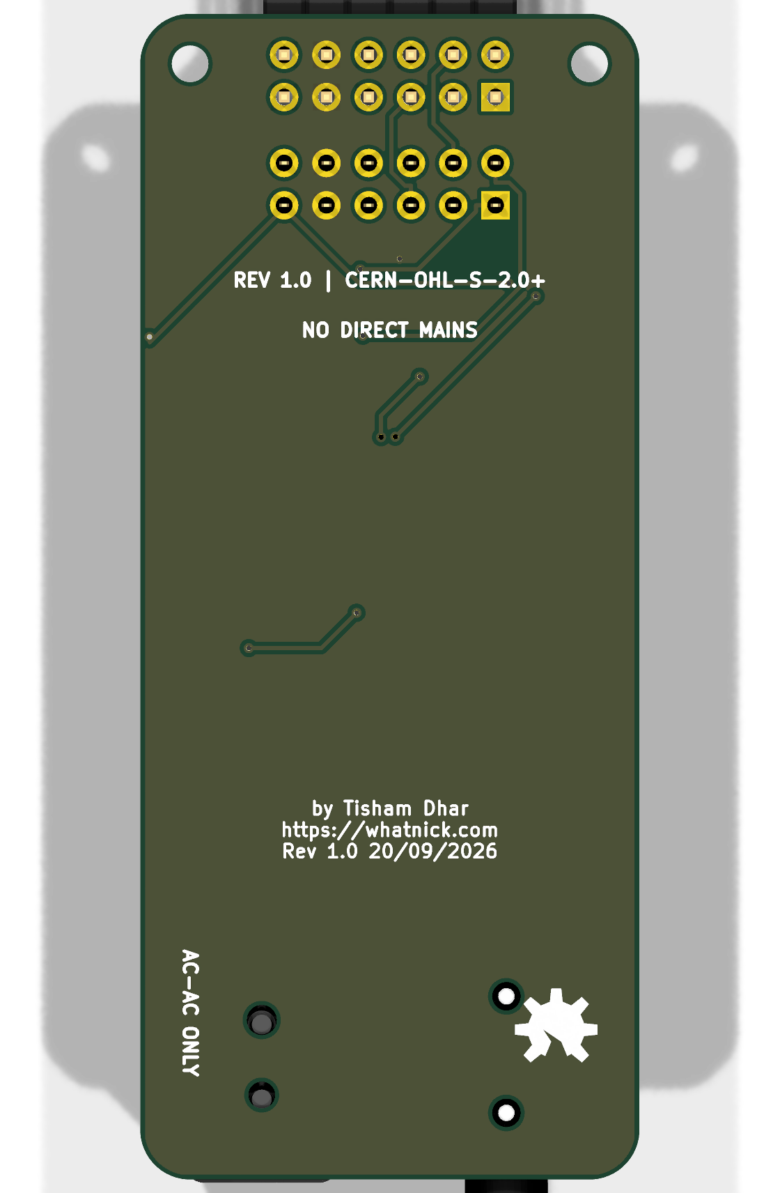
| Component side | Rear silkscreen and routing |
|---|---|
 |  |
The CTVT Energy DSP repository contains the companion Tiny Tapeout design. Its working first stage captures ADS131M02 frames, performs time-shared multiply-accumulate operations, generates the ADC clock and reset, and publishes coherent voltage, current, active-power, RMS, and energy measurements over a separate host SPI interface. The roadmap adds full ADC register configuration, gain/phase calibration, power-quality events, and resource-efficient Goertzel harmonic analysis.
See ADC PMOD comparative analysis for a
comparison with the commercial ADC and mixed-signal boards listed in
docs/expansion_boards__daughter_cards.csv,
including the AD7124-8 precision delta-sigma PMOD.
CT jack -> split burden -> protection -> differential RC filter --+
                                                                   |
AC/AC jack -> balanced divider -> protection -> differential RC ---+-> ADS131M02
                                                                        |
3.3 V PMOD <---------------- SPI, DRDY, RESET, CLK ----------------------+SJ-3523-SMT-TR 3.5 mm stereo jack, with
tip and sleeve as the differential CT input and ring grounded. Two 6.49 ohm
0.1% burden resistors form a 12.98 ohm differential burden. The jack's
mating face overhangs the field edge by 2.0 mm so a right-angle plug body
clears the PCB.PJ-002BH-SMT-TR barrel jack for an isolated
9-12 VAC transformer. Each leg uses a 100 kohm / 6.49 kohm balanced divider.SMF3.3CA on the CT input and SMBJ18CA on the transformer
input.J1 is the right-angle male peripheral connector. J4 is a vertical female
Wurth 61301221821 vertical pass-through socket; all twelve pins are connected
one-to-one for PMOD chaining.
| Pin | Signal | Direction at CTVT | Purpose |
|---|---|---|---|
| 1 | CS | Input | SPI chip select |
| 2 | MOSI | Input | SPI data to ADC |
| 3 | MISO | Output | SPI data from ADC |
| 4 | SCLK | Input | SPI clock |
| 5 | GND | Power | Ground |
| 6 | +3V3 | Power | Regulated 3.3 V input |
| 7 | DRDY | Output | Conversion-ready interrupt |
| 8 | RESET | Input | ADC reset |
| 9 | CLK_HOST | Input | Optional external ADC clock |
| 10 | RESERVED | Pass-through | Reserved chained signal |
| 11 | GND | Power | Ground |
| 12 | +3V3 | Power | Regulated 3.3 V input |
The Tiny Tapeout companion maps the PMOD signals as follows:
| PMOD signal | Tiny Tapeout signal |
|---|---|
| CS | uio[0] |
| MOSI | uio[1] |
| MISO | uio[2] |
| SCLK | uio[3] |
| DRDY | uio[4] |
| RESET | uio[5] |
| CLK_HOST | uio[6] |
This standard Pmod ordering lets the board plug directly into the bidirectional Tiny Tapeout/FabricFox connector. The host processor uses the separate input and output ports, so it does not contend with the ADC bus.
The CT channel differential voltage is:
V_CT_RMS = I_secondary_RMS x 12.98 ohmFor example, a 100 A : 50 mA CT produces approximately 0.649 Vrms at rated primary current. Confirm the selected CT's maximum secondary current and fault behavior before connection.
The voltage channel nominal divider ratio is:
6.49 kohm / (100 kohm + 6.49 kohm) = 0.06095A 9-12 Vrms isolated transformer therefore produces approximately 0.549-0.731 Vrms differential at the ADC input. Configure the ADS131M02 gain for the resulting peak voltage and retain headroom for transformer regulation and mains excursions.
Calibrate voltage gain, current gain, phase, and channel offset against a traceable low-voltage source before calculating power. TP1-TP4 expose the four ADC inputs; TP5 is DRDY, TP6 is +3V3, and TP7 is GND.
Use only an isolated CT and a certified isolated AC/AC transformer. Never connect mains directly to this board. The barrel jack is an isolated low-voltage AC input, not a DC supply input. Enclosure, wiring, fusing, creepage, clearance, and regulatory compliance remain the responsibility of the final system.
Open ctvt-pmod.kicad_pro in KiCad 10. The committed schematic and PCB are
complete and routed. Project-local connector footprints and STEP models avoid
dependencies on the ATM90E26 FeatherWing repository.
The design sources are generated in this order:
python scripts\generate_schematic.py
& "C:\Program Files\KiCad\10.0\bin\python.exe" scripts\generate_board.py
# Export a Specctra DSN, route it, and save the result as routing\ctvt-pmod.ses.
& "C:\Program Files\KiCad\10.0\bin\python.exe" scripts\finalize_route.py
scripts/finalize_route.py imports the saved Freerouting session, normalizes
all traces to at least 0.25 mm, verifies the stereo jack's generated 2.0 mm
mating-face overhang, adds the rear OSHW/Whatnick branding, and fills GND zones
on both copper layers. Run scripts\adjust_stereo_jack.py to verify the
overhang independently or
scripts\add_branding.py to reapply only the branding.
Run scripts\add_mechanical_features.py to reapply the 3 mm corner radii and
two M2 mounting holes without disturbing routed copper or manual silkscreen.
Manufacturing exports are generated into ignored gerbers/ and bom/
directories. The reviewed orderable BOM and DigiKey sourcing notes are
committed in docs/ctvt-pmod-sourced-bom.csv
and docs/bom-sourcing.md.
Generate the Elecrow PCBA upload package with:
python scripts\export_elecrow.pyThis creates manufacturing/elecrow/ctvt-pmod-elecrow-pcba.zip containing a
Gerber ZIP, curated BOM, component position file, and current KiCad DRC/ERC
reports. See
docs/elecrow-manufacturing.md for package
contents and assembly-review notes.
ctvt-pmod.kicad_sch - complete schematicctvt-pmod.kicad_pcb - routed two-layer PCBctvt-pmod.pretty/ - project-local barrel-jack and PMOD socket footprintsmodels/step/ - project-local connector STEP modelsrouting/ctvt-pmod.ses - saved autorouter resultscripts/ - deterministic schematic, placement, and routing finalizationLicensed under CERN-OHL-S-2.0-or-later.
| Qty | Value | Footprint | References |
|---|---|---|---|
| 4 | 1k 0.1% | R_0603_1608Metric | R3, R4, R9, R10 |
| 2 | 100k 0.1% | R_0805_2012Metric | R5, R6 |
| 2 | 100nF | C_0603_1608Metric | C4, C6 |
| 2 | 10k | R_0603_1608Metric | R11, R12 |
| 2 | 10nF C0G | C_0603_1608Metric | C1, C2 |
| 2 | 1uF | C_0603_1608Metric | C3, C5 |
| 2 | 6.49R 0.1% | R_0805_2012Metric | R1, R2 |
| 2 | 6.49k 0.1% | R_0805_2012Metric | R7, R8 |
| 2 | M2 mounting hole | MountingHole_2.2mm_M2 | H1, H2 |
| 1 | +3V3 | TestPoint_Pad_D1.0mm | TP6 |
| 1 | 220nF | C_0603_1608Metric | C7 |
| 1 | 33R | R_0603_1608Metric | R13 |
| 1 | 600R@100MHz | L_0603_1608Metric | FB1 |
| 1 | 61301221821 | PinSocket_2x06_P2.54mm_PMODHost1A | J4 |
| 1 | ADS131M02IPWR | TSSOP-20_4.4x6.5mm_P0.65mm | U1 |
| 1 | AIN0N | TestPoint_Pad_D1.0mm | TP2 |
| 1 | AIN0P | TestPoint_Pad_D1.0mm | TP1 |
| 1 | AIN1N | TestPoint_Pad_D1.0mm | TP4 |
| 1 | AIN1P | TestPoint_Pad_D1.0mm | TP3 |
| 1 | DRDY | TestPoint_Pad_D1.0mm | TP5 |
| 1 | GND | TestPoint_Pad_D1.0mm | TP7 |
| 1 | OSHW-LOGO-M | OSHW-LOGO-M | LOGO1 |
| 1 | PJ-002BH-SMT-TR | DC_BARREL_JACK_SMD_2MM | J3 |
| 1 | SJ-3523-SMT-TR | Jack_3.5mm_CUI_SJ-3523-SMT_Horizontal | J2 |
| 1 | SMBJ18CA | D_SMB | D2 |
| 1 | SMF3.3CA | D_SOD-123F | D1 |
| 1 | Tiny Tapeout PMOD | PinHeader_2x06_P2.54mm_Horizontal | J1 |
| 1 | Whatnick_logo | Whatnick_logo | LOGO2 |
It measures 30 × 70 mm and has 2 copper layers, 1.6 mm thick.
39 parts, built around the PJ-002BH-SMT-TR, SJ-3523-SMT-TR, SMBJ18CA and SMF3.3CA. The full list of its parts is on this page, with links to each part's symbol and footprint where PCBKit's library has them.
From the whatnick/ctvt-pmod repository on GitHub, at the commit this page was made from: the board is ctvt-pmod.kicad_pcb and its schematic ctvt-pmod.kicad_sch. PCBKit opens the board in the browser, with nothing to install.
Its repository states no licence, so its author keeps all rights: ask whatnick before reusing the design.


igorwolfs/modular-processing-hw
MCU Breakout board with Hirose BM28B connector


lessthan00/AMS1117_3V3
VIN 18V VOUT 3.3V IOUT 1A package SOT-223 IQ 12mA VD 1.4V@1A


