2 layers35 × 50 mm

 wallago/kagu
ZMK firmware for a handwired wireless split keyboard on Seeed XIAO nRF52840.
Kagu is an open-source printed circuit board by wallago, from the wallago/kagu repository on GitHub, published under the Apache-2.0 licence. It is a 2-layer board of 127 × 91.5 mm with 60 parts on 47 nets, routed with 325 tracks and 30 vias.
Its parts include 19 switches, 18 diodes, 1 resistor and 1 IC. It belongs with the keyboards and input boards and the nRF52 and nRF5x boards of this library.
A wireless 36-key split keyboard (3x5+3) on the Seeed XIAO nRF52840, running ZMK.
keymap.txt: the keymap, the only file to edit for layout changeskeymap/: the generator that turns it into ZMK, and the diagramconfig/: ZMK shields and the generated kagu.keymappcb/: KiCad projects for both halvescase/: OpenSCAD trays, top plates and Choc v2 keycap risers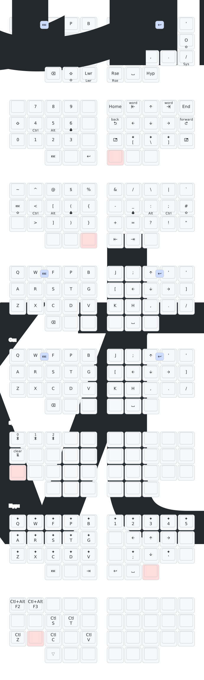
Colemak-DH, after dubu36. Shortcut modifiers sit on the home row (pinky to index: Shift, Ctrl, Alt, Super, mirrored). Shift and the layers you use while writing sit on the thumbs, which keeps hold-tap timing out of the way. Some notes on the layers:
, (app) or D and H (os). They keep Ctrl or Super down for
the whole hold, so every key is sent with that modifier, including the arrows on U N E I./.Each layer is a grid of the 36 keys, laid out as they sit on the board: three rows of ten, then the six thumbs.
layer base: left_mods, right_mods
  Q      W        F      P     B          J        L     U      Y     '
  A      R        S      T     G          M        N     E      I     O
  Z/sys  X/mou    C/app  D/os  V          K        H/os  ,/app  .     \//sys
BSPC LSHFT/LSHFT lwr/lwr rse/rse SPC _/hyp Z/sys tap Z, hold the sys layer
T/LGUI:hm tap T, hold Super, as a positional home-row mod
LSHFT/LSHFT one-shot Shift on tap, plain Shift on hold
_ / TRNS nothing / fall through to the layer belowHolds shared by several layers are written once as an overlay and listed after the layer name.
layer app + LCTRL holds Ctrl for as long as the layer is held. Combos are written
W F -> ESC. The header of keymap.txt covers the details.
After editing, run just keymap in the Nix dev shell. It regenerates kagu.keymap and redraws
the diagram with keymap-drawer. CI fails if
kagu.keymap is out of date.
| Qty | Value | Footprint | References |
|---|---|---|---|
| 18 | D | kagu:D_SOD-123 | D1, D2, D3, D4, D5, D6, D7, D10, D11, D12, D13, D14, D15, D16, D17, D18 +2 |
| 18 | SW_Push | PCM_Switch_Keyboard_Hotswap_Kailh:SW_Hotswap_Kailh_Choc_V1V2_Plated | SW1, SW2, SW3, SW4, SW5, SW6, SW7, SW10, SW11, SW12, SW13, SW14, SW15, SW16, SW17, SW18 +2 |
| 13 | Conn_01x01_Pin | kagu:TestPad | Bat_HW1, GND_HW1, I2S_SCK1, I2S_SD1, I2S_WS1, NFC_1, NFC_2, RESET_HW1, SPI_MISO1, SPI_MOSI1, SPI_SCK1, UART_RX1, UART_TX1 |
| 5 | MountingHole | MountingHole:MountingHole_3.2mm_M3_DIN965_Pad | H1, H2, H4, H5, H6 |
| 2 | Conn_01x02_Pin | Connector_JST:JST_PH_S2B-PH-SM4-TB_1x02-1MP_P2.00mm_Horizontal | Bat_Con1, Switch_Con1 |
| 1 | Conn_01x02_Pin | Connector_JST:JST_SH_SM02B-SRSS-TB_1x02-1MP_P1.00mm_Horizontal | Bat_LED_Con1 |
| 1 | R(1k) | Resistor_SMD:R_0805_2012Metric | R1 |
| 1 | SW_Push | Button_Switch_SMD:SW_Push_SPST_NO_Alps_SKRK | SW19 |
| 1 | XIAO-nRF52840-Plus-SMD | XIAO nRF52840:XIAO-23P-Add-On-Plus | U1 |
It measures 127 × 91.5 mm and has 2 copper layers, 1.6 mm thick.
60 parts. The full list of its parts is on this page, with links to each part's symbol and footprint where PCBKit's library has them.
From the wallago/kagu repository on GitHub, at the commit this page was made from: the board is pcb/kagu-left/kagu.kicad_pcb and its schematic pcb/kagu-left/kagu.kicad_sch. PCBKit opens the board in the browser, with nothing to install.
Its repository publishes it under the Apache-2.0 licence: you may reuse it on that licence's terms (keep the author's notice, and for a copyleft licence share your changes alike).


sd2psx/pcb
The PCB must be produced in 0.8mm thickness. Production files are provided under the "Releases" tab. These do not include the through-hole OLED module.


BitDogLab/BitDogLab
Open-source educational hardware for embedded systems, programming, electronics, and physical computing.