2 layers48 × 60 mm
Custom wireless mouse
limmjacc/custom-wireless-mouse
Project to track the hardware and firmware for a custom made computer mouse.
33 parts

 Vipin1113/smart-ring-project
Compact BLE-Based Smart Ring PCB for Health Monitoring and Gesture Detection
Prj kicad is an open-source printed circuit board by Vipin1113, from the Vipin1113/smart-ring-project repository on GitHub, published under the MIT licence. It is a 2-layer board of 22.8 × 9.6 mm with 38 parts on 43 nets, routed with 286 tracks and 38 vias.
It is built around the NRF52810-QCAA-T, MAX30102 and 2450AT18A100E, with the ICM-42670-P, TPS78233DDCR and ECS-320-8-37-CKM-TR3 among its other parts. Its parts include 21 capacitors, 6 ICs, 5 resistors, 4 connectors and 1 inductor. It belongs with the radio and wireless boards and the nRF52 and nRF5x boards of this library.


This repository contains the complete KiCad project files, PCB layouts, schematic designs, manufacturing outputs, and documentation for a compact BLE-enabled Smart Ring developed for health monitoring and gesture detection applications.
The project focuses on wearable-oriented PCB miniaturization, low-power BLE communication, physiological sensing, gesture detection, RF-aware PCB implementation, and compact embedded system integration within a smart-ring-compatible form factor.
The implemented smart ring integrates:
The final PCB dimensions achieved are:
22.8 mm × 9.6 mm
| Component | Manufacturer | Part Number |
|---|---|---|
| BLE MCU | Nordic Semiconductor | nRF52810-QCAA-T |
| PPG Sensor | Analog Devices | MAX30102 |
| IMU Sensor | TDK InvenSense | ICM-42670-P |
| Battery Charging IC | Microchip Technology | MCP73831-2-OT |
| 3.3V LDO | Texas Instruments | TPS78233DDC |
| 32 MHz Crystal | ECS Inc. | ECS-320-8-37-CKM-TR |
| 2.4 GHz Antenna | Johanson Technology | 2450AT18A100E |
The initial smart ring implementation utilized a larger PSoC BLE module-based architecture which occupied approximately:
30.4 mm × 12.0 mm
Although the module simplified BLE integration, it significantly increased PCB area and routing constraints.
To improve compactness and wearable compatibility, the architecture was migrated to the Nordic nRF52810 BLE SoC in a compact QFN package.
After multiple PCB iterations and routing optimizations, the final PCB dimensions were successfully reduced to:
22.8 mm × 9.6 mm
Major optimizations implemented include:
Commercial smart-ring products generally utilize advanced packaging and PCB technologies including:
Industrial wearable PMIC solutions analyzed during this project include:
These PMICs integrate:
within a single compact package.
Although such PMICs can significantly reduce PCB area, they introduce substantially higher routing complexity and manufacturing difficulty. Therefore, a simpler discrete charging and regulation architecture was selected for the current implementation.
smart-ring-project/
├── README.md
├── LICENSE
├── smart_ring.kicad_pro
├── smart_ring.kicad_sch
├── smart_ring.kicad_pcb
├── Gerbers/
├── Images/
├── Report/
└── Datasheets/
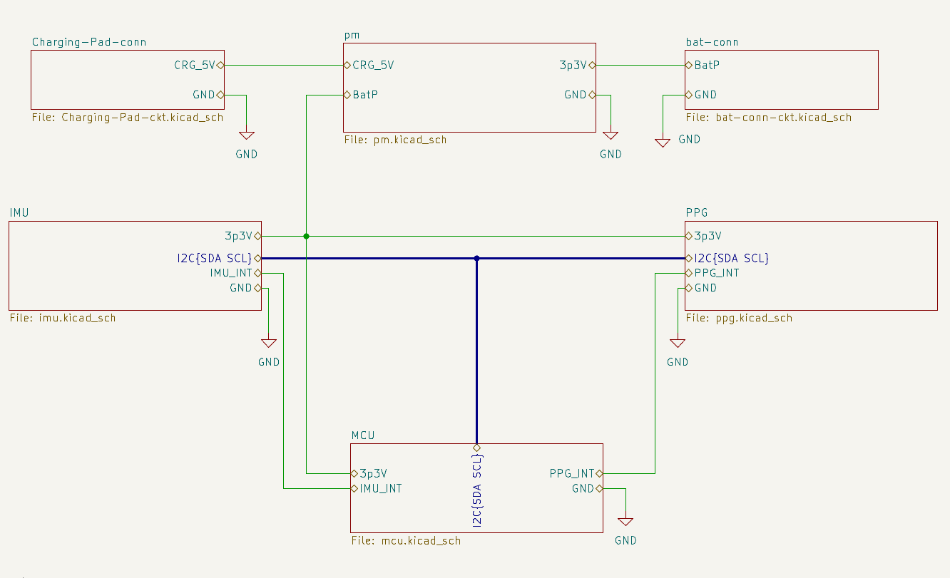
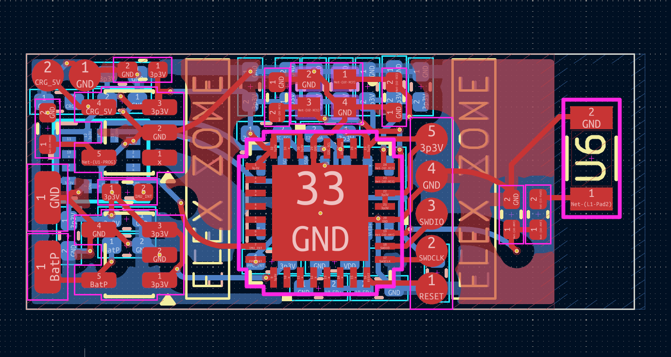
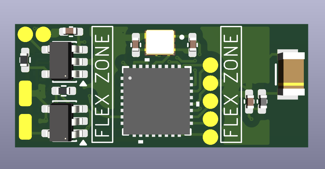
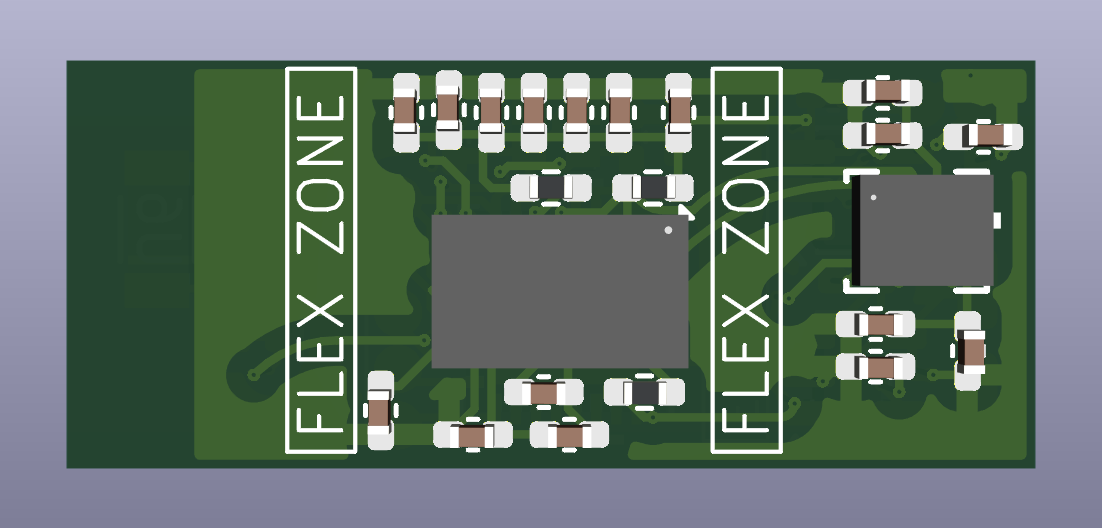
The implemented smart ring PCB successfully passed:
The design additionally incorporates:
Future improvements may include:
This project is licensed under the MIT License.
See the LICENSE file for details.
Vipin Kumar Mishra
M.Tech ECE (VLSI)
IIIT Bangalore
This project was developed as part of the Electronic Systems Packaging course project focusing on compact wearable embedded system design, PCB miniaturization, RF-aware layout implementation, and smart wearable hardware development.
| Qty | Value | Footprint | References |
|---|---|---|---|
| 10 | 0.1u | Capacitor_SMD:C_0402_1005Metric_Pad0.74x0.62mm_HandSolder | C5, C6, C7, C10, C11, C14, C16, C18, C19, C22 |
| 5 | 1u | Capacitor_SMD:C_0402_1005Metric_Pad0.74x0.62mm_HandSolder | C1, C2, C3, C15, C21 |
| 3 | 4.7u | Capacitor_SMD:C_0402_1005Metric_Pad0.74x0.62mm_HandSolder | C4, C8, C17 |
| 2 | 10K | Resistor_SMD:R_0402_1005Metric_Pad0.72x0.64mm_HandSolder | R4, R8 |
| 2 | 12p | Capacitor_SMD:C_0402_1005Metric_Pad0.74x0.62mm_HandSolder | C12, C13 |
| 2 | 4.7K | Resistor_SMD:R_0402_1005Metric_Pad0.72x0.64mm_HandSolder | R6, R7 |
| 2 | Conn_01x01 | Connector_Wire:SolderWirePad_1x01_SMD_1x2mm | J1, J2 |
| 1 | 0.8p | Capacitor_SMD:C_0402_1005Metric_Pad0.74x0.62mm_HandSolder | C9 |
| 1 | 2450AT18A100E | SR_Library:2450AT18A100E_JOT | U6 |
| 1 | 3.9n | Inductor_SMD:L_0402_1005Metric_Pad0.77x0.64mm_HandSolder | L1 |
| 1 | 40K | Resistor_SMD:R_0402_1005Metric_Pad0.72x0.64mm_HandSolder | R1 |
| 1 | Conn_01x02 | SR_Library:Charging_Pad | J3 |
| 1 | Conn_01x05 | SR_Library:SWD_Pad | J4 |
| 1 | ECS-320-8-37-CKM-TR | SR_Library:XTAL_ECS-320-8-37-CKM-TR | Y2 |
| 1 | ICM-42670-P | SR_Library:LGA14_2.5X3X0.76_IVS | U3 |
| 1 | MAX30102 | OptoDevice:Maxim_OLGA-14_3.3x5.6mm_P0.8mm | U5 |
| 1 | MCP73831-2-OT | Package_TO_SOT_SMD:SOT-23-5 | U1 |
| 1 | NRF52810-QCAA-T | SR_Library:QFN32_5X5_NOR | U2 |
| 1 | TPS78233DDC | Package_TO_SOT_SMD:SOT-23-5 | U4 |
It measures 22.8 × 9.6 mm and has 2 copper layers, 1.6 mm thick.
38 parts, built around the NRF52810-QCAA-T, MAX30102, 2450AT18A100E and ICM-42670-P. The full list of its parts is on this page, with links to each part's symbol and footprint where PCBKit's library has them.
From the Vipin1113/smart-ring-project repository on GitHub, at the commit this page was made from: the board is prj-kicad.kicad_pcb and its schematic prj-kicad.kicad_sch. PCBKit opens the board in the browser, with nothing to install.
Its repository publishes it under the MIT licence: you may reuse it on that licence's terms (keep the author's notice, and for a copyleft licence share your changes alike).
limmjacc/custom-wireless-mouse
Project to track the hardware and firmware for a custom made computer mouse.


Reekoru/STM32WB55REV6_Board
A dev board for STM32WB55REV6 that includes RF for Bluetooth / LE, Thread, & Zigbee. Includes GPIO ports, ST-Link via TC2030 by Tag Connect, and USB-UART

souhaib250/SENS-CO-Wearable-Gas-Sensor
Design, simulation and PCB implementation of an embedded wireless acquisition node for a wearable WS2 gas sensor.