2 layers103 × 30.5 mm
 Veger1/LAB2
Alignment tool ============== Download Main.exe from the latest release. Opening Main.exe may open console depending on version, then the application will start.
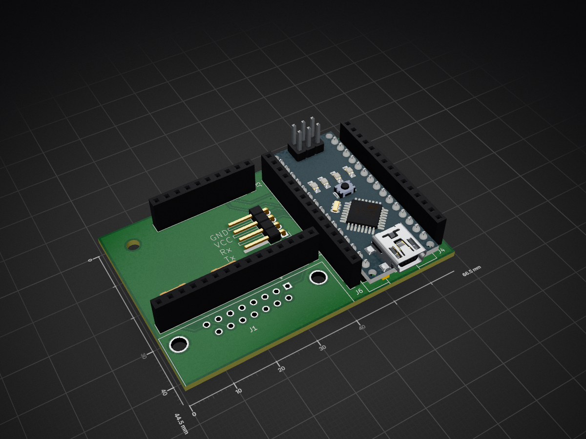
LAB2 is an open-source printed circuit board by Veger1, from the Veger1/LAB2 repository on GitHub. It is a 2-layer board of 66.5 × 44.5 mm with 9 parts on 48 nets, routed with 127 tracks and 2 vias.
Its parts include 6 connectors and 2 resistors. It belongs with the AVR (ATmega, ATtiny) boards of this library.
Download Main.exe from the latest release. Opening Main.exe may open console depending on version, then the application will start.
Known issues: v1.3.0 and below:
v1.2.0 and below:
v1.1.0 and below:
| Qty | Value | Footprint | References |
|---|---|---|---|
| 2 | Conn_01x15_Socket | Connector_PinSocket_2.54mm:PinSocket_1x15_P2.54mm_Vertical | J4, J6 |
| 2 | R | Resistor_THT:R_Axial_DIN0207_L6.3mm_D2.5mm_P7.62mm_Horizontal | R1, R2 |
| 1 | Arduino_Nano_v3.x | Module:Arduino_Nano | A2 |
| 1 | Conn_01x04_Pin | Connector_PinHeader_2.54mm:PinHeader_1x04_P2.54mm_Horizontal | J2 |
| 1 | Conn_01x10_Socket | Connector_PinSocket_2.54mm:PinSocket_1x10_P2.54mm_Vertical | J3 |
| 1 | Conn_01x15_Socket_SubD15_Header | Connector_PinSocket_2.54mm:PinSocket_1x15_P2.54mm_Vertical | J5 |
| 1 | DA15_Receptacle_MountingHoles | Connector_Dsub:DSUB-15_Female_Horizontal_P2.77x2.84mm_EdgePinOffset9.90mm_Housed_MountingHolesOffset11.32mm | J1 |


FrameworkComputer/ExpansionCards
Reference designs and documentation to create Expansion Cards for the Framework Laptop

VoronDesign/Voron-Hardware
Cool Hardware designed by the Voron Design group

hackclub/OnBoard
💡 Join 1,000 teenagers and make your first PCB with a $100 grant!


adamws/kicad-kbplacer
KiCad plugin for automatic keyboard's key placement and routing
It measures 66.5 × 44.5 mm and has 2 copper layers, 1.6 mm thick.
9 parts. The full list of its parts is on this page, with links to each part's symbol and footprint where PCBKit's library has them.
From the Veger1/LAB2 repository on GitHub, at the commit this page was made from: the board is KiCAD/V2/V2.kicad_pcb and its schematic KiCAD/V2/V2.kicad_sch. PCBKit opens the board in the browser, with nothing to install.
Its repository states no licence, so its author keeps all rights: ask Veger1 before reusing the design.