4 layers230.7 × 97.8 mm

 vadikgo/EC60_origin
Open source universal 60% Electrostatic Capacitive PCB.
EC60-Rev 1 1 1 is an open-source printed circuit board by vadikgo, from the vadikgo/EC60_origin repository on GitHub, published under the MIT licence. It is a 4-layer board of 285 × 94.6 mm with 157 parts on 68 nets, routed with 1,000 tracks and 488 vias.
It is built around the OPA350UA, 74HC4051 and PRTR5V0U2X, with the TYPEC-304YSSW-ACP16 among its other parts. Its parts include 75 switches, 28 resistors, 13 capacitors, 5 ICs and 1 diode. It belongs with the STM32 boards of this library.


Open source universal 60% Electrostatic Capacitive PCB.
This project is a continuation of my development of open source EC boards.
The supported layout options are the following:
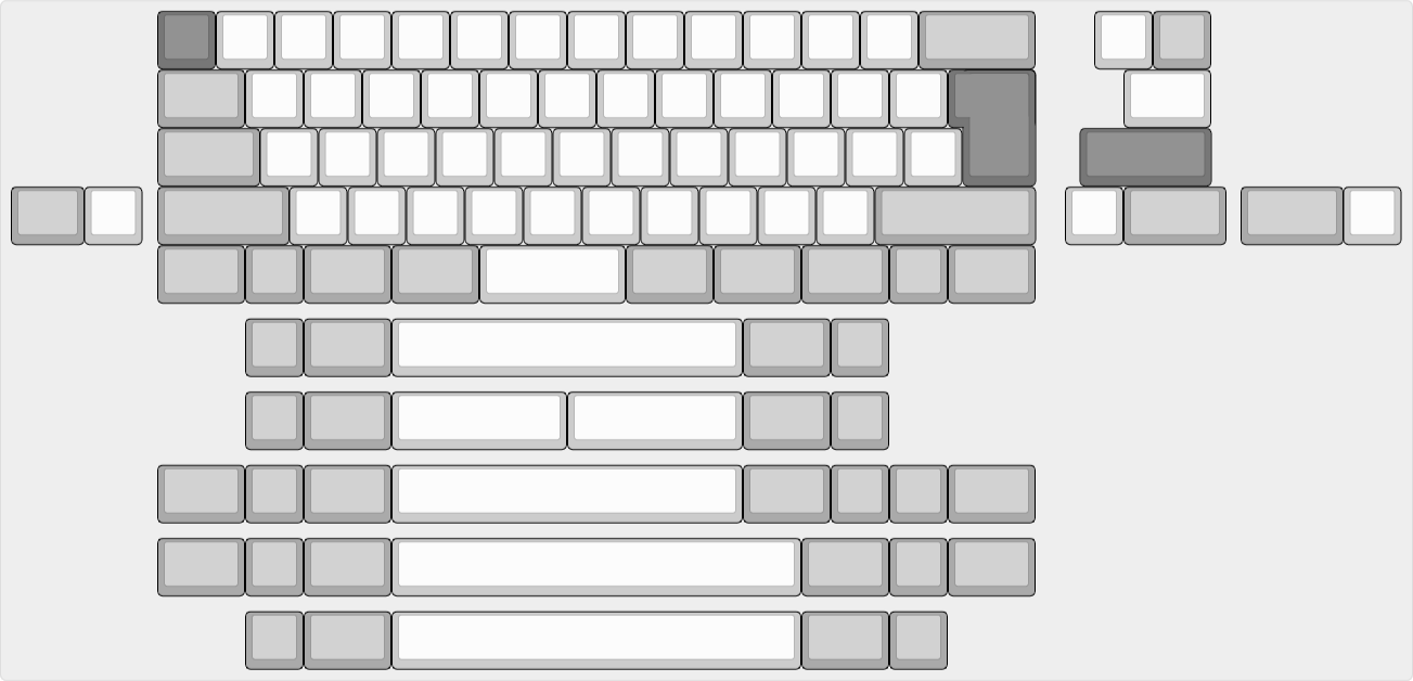
Mapping is purely for demonstration purposes, remapping of all keys is supported.
Mainboard:
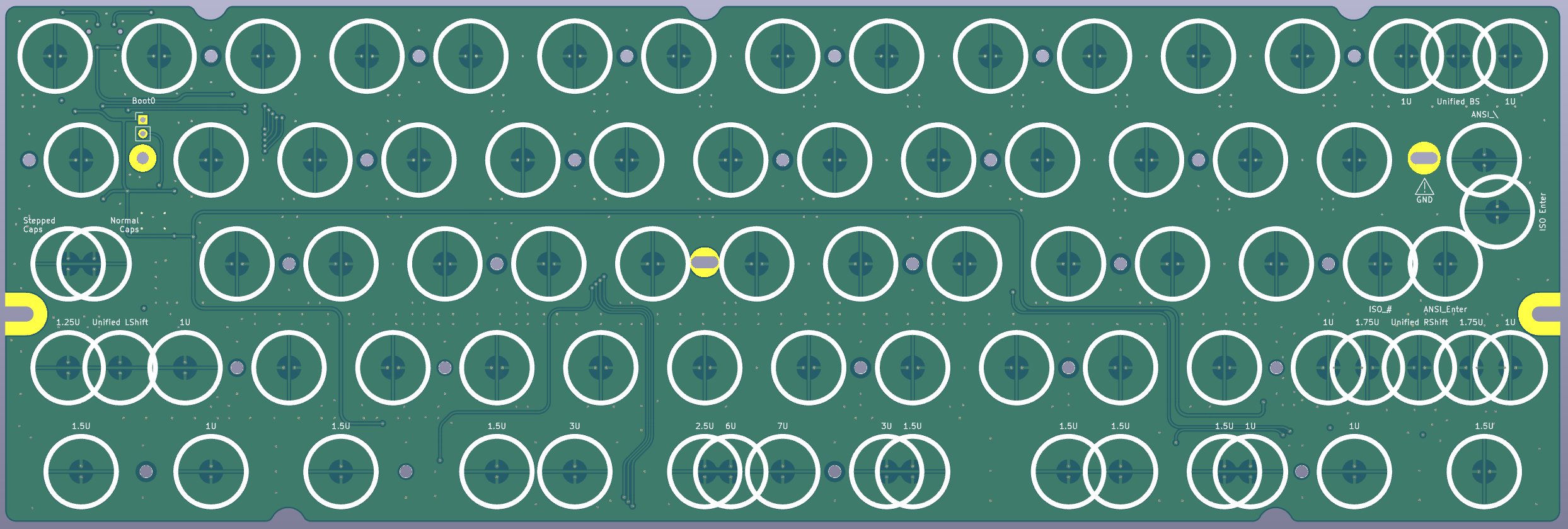
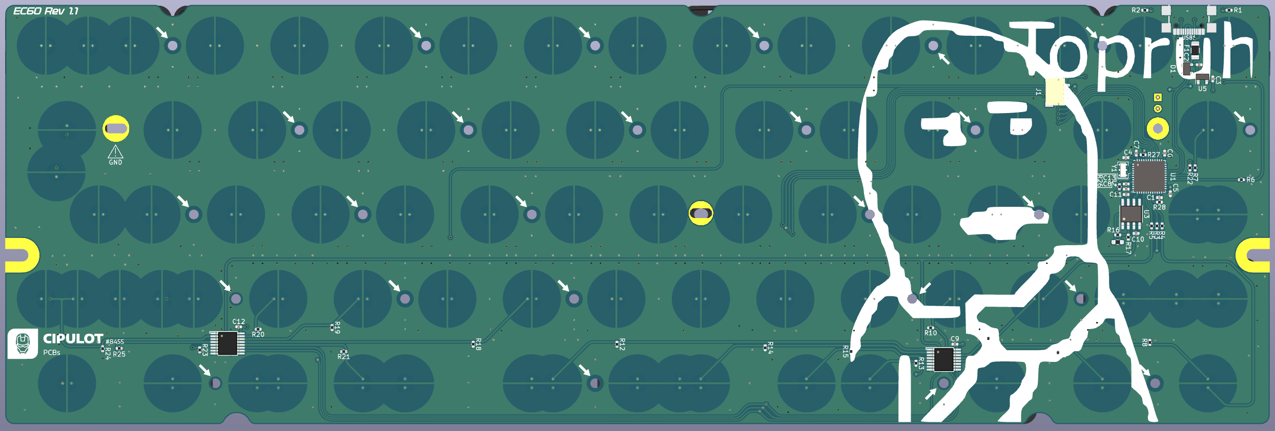
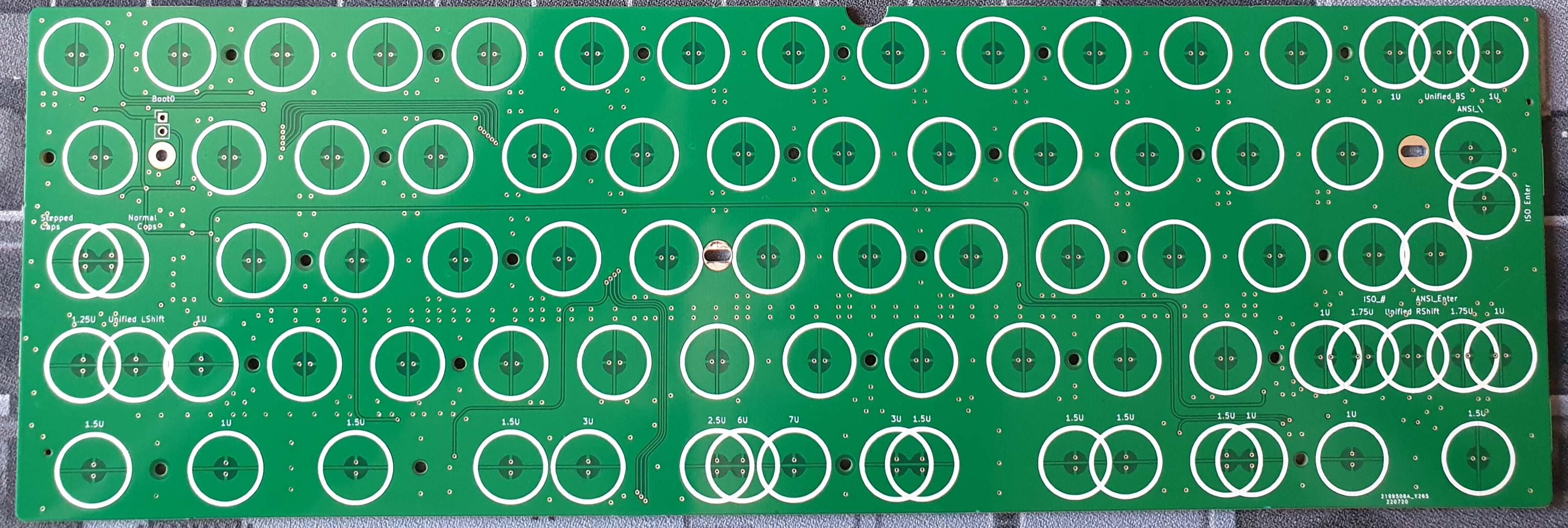
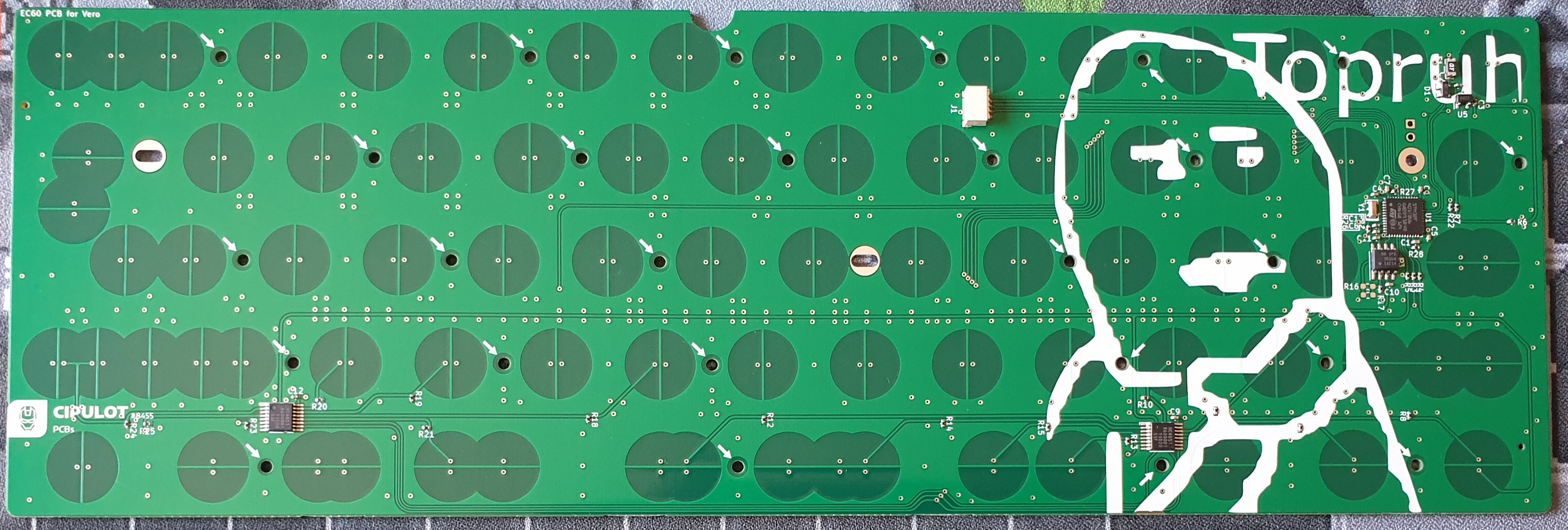
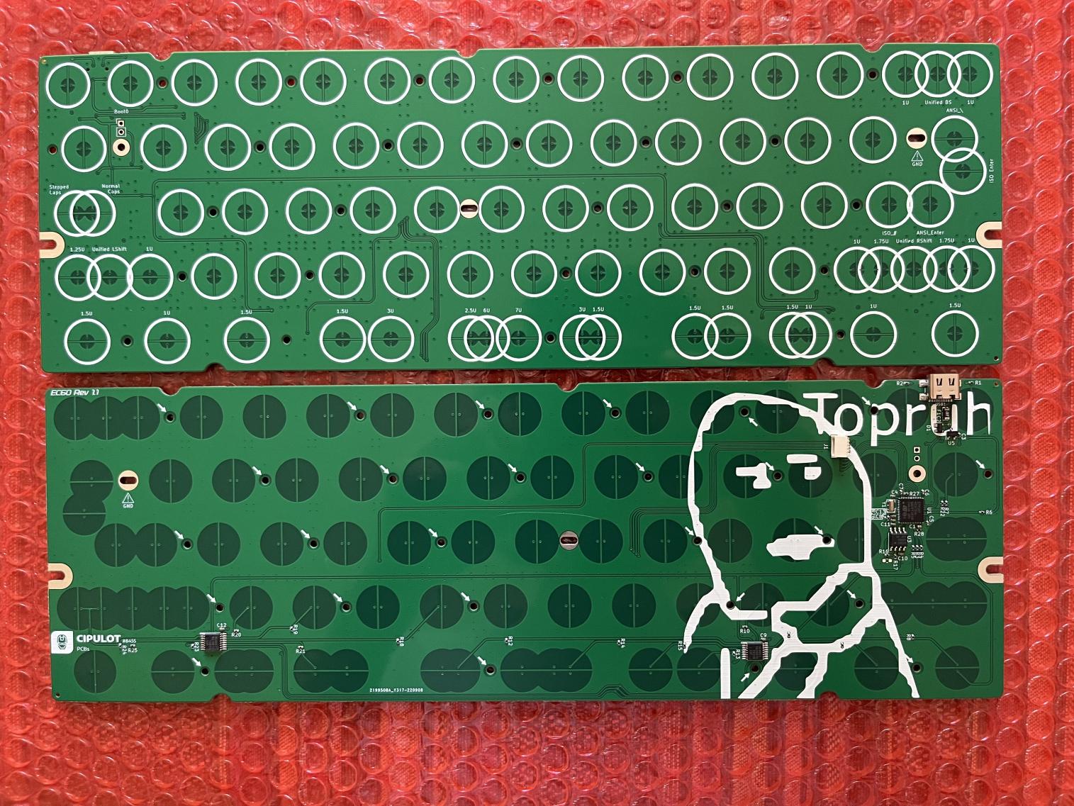
NOTE: the prototype PCB for Rev1 doesn't include a USB port and the JST connector is in a different position compared to the one in the render. This is because the above was a modified version of the PCB to be used in Vero. For all intents and purposes, the PCB is the same.
This revision implements all the main features of the PCB.
This revision implements some changes:
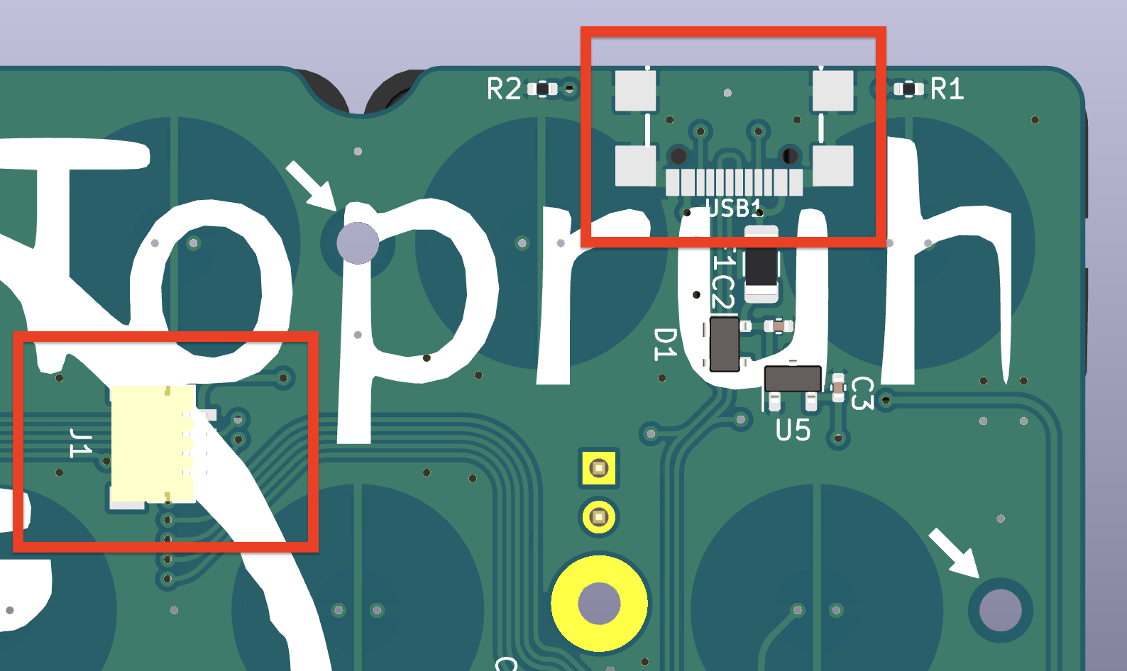
Both onboard USB-C and JST connectors are supported. In both cases the protection features are preserved (fused and ESD).
In order to have me highers compatibility possible with PCB manufacturers, I decided to design the board around the JLC7628 Stackup from JLCPCB.
The rational behind this is that the JCPCB stackup is relatively cheap and if the board worked with the stackup, it would be easier to get the board to work with pretty much any other many that offer an equivalent stackup and higher prices.
The production can be found in the Production folder.
As usual the *.zip files are the gerber files, BOM-*.csv are the BOM (Bill Of Material) files and POS-*.csv are the POS/CPL (Footprint POSition/Component Placement List) files.
As mentioned above, the mainboard is designed around the JLCPCB stackup. The mainboard is a 4 layer board.
Here are the options to select when ordering the mainboard:
EC60-F_Cu.gbrEC60-In1_Cu.gbrEC60-In2_Cu.gbrEC60-B_Cu.gbrFR-4 TG155All the other options can be left as default.
Here follows the options to be used for assembly:
Added by JLCPCByesNOTES ABOUT THE OPTIONS
Once you upload the gerber files wait for the system to automatically recognize the board outline and layers. It will take a while, be patient.
PCB thickness has been tested on both 1.6mm and 1.2mm so it's your call on which one to use.
For Material Type I strongly suggest to use FR-4 TG155, using the standard FR4-Standard TG130-140 material might result in the board delamination and generally is not advised on 4 layer boards.
This project is released under the MIT License. For the license, please refer to the LICENSE.md file.
| Qty | Value | Footprint | References |
|---|---|---|---|
| 60 | EC_SW | cipulot_parts:ecs_pad_1U_no_ring | SW2, SW10, SW11, SW12, SW13, SW14, SW15, SW17, SW18, SW19, SW20, SW21, SW22, SW23, SW24, SW25 +44 |
| 26 | MountingHole | cipulot_parts:HOLE_M2 | H1, H2, H10, H11, H12, H13, H14, H15, H16, H17, H18, H19, H20, H21, H22, H23 +10 |
| 17 | 100k | Resistor_SMD:R_0402_1005Metric | R8, R10, R11, R12, R13, R14, R15, R16, R18, R19, R20, R21, R22, R23, R24, R25 +1 |
| 8 | 100n | Capacitor_SMD:C_0402_1005Metric | C4, C5, C6, C7, C8, C9, C11, C12 |
| 5 | 100 | Resistor_SMD:R_0402_1005Metric | R3, R4, R5, R6, R7 |
| 4 | EC_SW | cipulot_parts:ecs_pad_0.25U_spaced_no_ring | SW33, SW68, SW69, SW71 |
| 3 | 10k | Resistor_SMD:R_0402_1005Metric | R26, R27, R28 |
| 3 | 1u | Capacitor_SMD:C_0402_1005Metric | C2, C3, C13 |
| 2 | 5.1k | Resistor_SMD:R_0402_1005Metric | R1, R2 |
| 2 | 74HC4051 | cipulot_parts:TSSOP16 | U2, U4 |
| 2 | EC_SW | cipulot_parts:ecs_pad_2U_no_ring | SW16, SW61 |
| 2 | EC_SW_1u&1.75u | cipulot_parts:ecs_pad_2.666U_spaced_no_ring_vertical | SW60, SW62 |
| 1 | 1k | Resistor_SMD:R_0402_1005Metric | R17 |
| 1 | 220p | Capacitor_SMD:C_0402_1005Metric | C10 |
| 1 | 4.7u | Capacitor_SMD:C_0402_1005Metric | C1 |
| 1 | 500mA | Fuse:Fuse_1206_3216Metric | F1 |
| 1 | 8 MHz | Crystal:Resonator_SMD_Murata_CSTxExxV-3Pin_3.0x1.1mm | Y1 |
| 1 | ANSI_Enter | cipulot_parts:ecs_pad_2U_no_ring | SW46 |
| 1 | ANSI_\ | cipulot_parts:ecs_pad_1U_no_ring | SW31 |
| 1 | BOOT0 | Connector_PinHeader_2.54mm:PinHeader_1x02_P2.54mm_Vertical | SW1 |
| 1 | EC_SW | cipulot_parts:ecs_pad_2U_no_ring_cut | SW48 |
| 1 | EC_SW | cipulot_parts:ecs_pad_1U_no_ring_1u_edge_cut | SW49 |
| 1 | Ext_Res | Resistor_SMD:R_0603_1608Metric_Pad0.98x0.95mm_HandSolder | JP1 |
| 1 | ISO_Enter | cipulot_parts:ecs_pad_2U_no_ring | SW32 |
| 1 | ISO_| | cipulot_parts:ecs_pad_1U_no_ring | SW45 |
| 1 | JST | cipulot_parts:JST-SR-4 | J1 |
| 1 | LOGO | cipulot_parts:Cipulot_Logo_Silk | G*** |
| 1 | OPA350 | Package_SO:SOIC-8_3.9x4.9mm_P1.27mm | U3 |
| 1 | PRTR5V0U2X | Package_TO_SOT_SMD:SOT-143 | D1 |
| 1 | STM32F401CBUx | Package_DFN_QFN:QFN-48-1EP_7x7mm_P0.5mm_EP5.6x5.6mm | U1 |
| 1 | TYPEC-304YSSW-ACP16 | cipulot_parts:TYPEC-304YSSW-ACP16 | USB1 |
| 1 | XC6206PxxxMR | Package_TO_SOT_SMD:SOT-23 | U5 |
The 154 most common of 157 parts.
It measures 285 × 94.6 mm and has 4 copper layers, 1.59 mm thick.
157 parts, built around the OPA350UA, 74HC4051, PRTR5V0U2X and TYPEC-304YSSW-ACP16. The full list of its parts is on this page, with links to each part's symbol and footprint where PCBKit's library has them.
From the vadikgo/EC60_origin repository on GitHub, at the commit this page was made from: the board is PCB/Rev_1_1_1/EC60-Rev_1_1_1.kicad_pcb and its schematic PCB/Rev_1_1_1/EC60-Rev_1_1_1.kicad_sch. PCBKit opens the board in the browser, with nothing to install.
Its repository publishes it under the MIT licence: you may reuse it on that licence's terms (keep the author's notice, and for a copyleft licence share your changes alike).


4pplet/EC-Pro-2
Open source replacement PCB kit for the HHKB Pro 2 keyboard.

4pplet/RF_R1_8-9Xu
Open source universal PCB for the Realforce R1 family of keyboards.