2 layers50 × 50 mm
Filmolino
filmolino/SlideScanner
The Filmolino SlideScanner is a device that makes it easy to scan slides in magazines fully automated using a modified slide projector and a digital camera.
37 parts28GPL-3.0
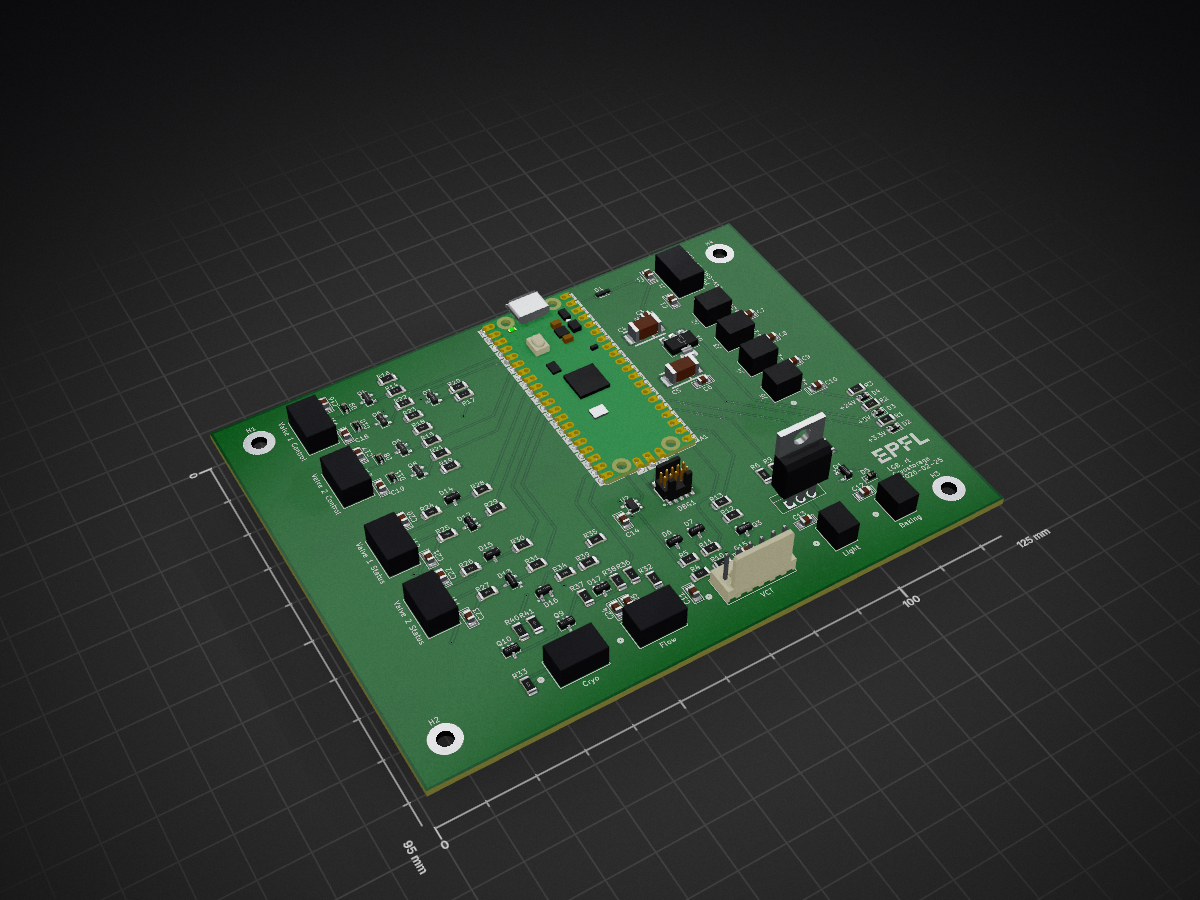
 trappitsch/cryostorage
This repository holds documentation, code, and hardware designs to control the cryostorage chamber. The purpose of this chamber is to allow storing of frozen samples in between characterization and analysis runs.
Cryostorage controller v1 is an open-source printed circuit board by trappitsch, from the trappitsch/cryostorage repository on GitHub, published under the MIT licence. It is a 2-layer board of 125 × 95 mm with 116 parts on 89 nets, routed with 400 tracks and 13 vias.
It is built around the SN74LVC1G04DBVR, BZX84C3V6 and 1N5819WS, with the AO3400A, BSS138 and FTSH-105-01-L-DV-K among its other parts. Its parts include 41 resistors, 25 capacitors, 17 diodes, 14 connectors and 10 transistors. It belongs with the RP2040 boards of this library.


This repository holds documentation, code, and hardware designs to control the cryostorage chamber. The purpose of this chamber is to allow storing of frozen samples in between characterization and analysis runs. The cryostorage chamber can hold eight sample holders and stores the samples at around 120 K in ultra-high vacuum.
While this project is highly specific to one specific hardware setup, I very much hope that parts of it can be used for other projects or at least, that the integration and overall idea can be helpful for you!
The documentation in the folder docs
contains the administrator documentation.
It thus describes the inner workings of the control hard- and software,
but does not really give a user guide on how to run it.
The deployed webpage of the documentation can be found at
https://trappitsch.github.io/cryostorage.
The design files for the PCB that controls all instruments that do not have
a direct computer interface (i.e., RS-232, USB, or Ethernet)
can be found in the pcb_controller folder.
PDF documents of previous schematics are hosted in the
previous_schematics folder.
All firm- and software crates can be found in the controller subfolder.
The important subfolders here are:
host: Contains the software that runs on the Reterminal and communicates
with the controller firmware.icd: Contains the shared types.firmware: Contains the firmware that runs on the Raspberry Pi Pico 2,
which runs the hardware PCB.While this projects rely on many open-source libraries, I would like to acknowledge three key parts without which this would not have been possible:

| Qty | Value | Footprint | References |
|---|---|---|---|
| 23 | 100nF | EasyEDA:CAP-SMD_L3.2-W1.6-FD-1 | C1, C2, C10, C11, C12, C13, C14, C15, C16, C17, C18, C19, C20, C21, C22, C23 +7 |
| 11 | 100kΩ | PCM_JLCPCB:R_1206 | R8, R9, R13, R16, R17, R18, R19, R23, R38, R39, R41 |
| 10 | 1kΩ | PCM_JLCPCB:R_1206 | R6, R7, R12, R14, R15, R20, R21, R22, R37, R40 |
| 9 | 100Ω | PCM_JLCPCB:R_1206 | R1, R5, R11, R28, R29, R30, R31, R35, R36 |
| 8 | 10kΩ | PCM_JLCPCB:R_1206 | R4, R10, R24, R25, R26, R27, R32, R33 |
| 8 | BZX84C3V6 | Package_TO_SOT_SMD:SOT-23 | D6, D7, D12, D13, D14, D15, D16, D17 |
| 7 | 22112042 | Snapeda:CONN_A-6373-04A_MOL | J1, J9, J10, J11, J12, J13, J14 |
| 6 | 22112022 | Snapeda:CONN_A-6373-02A_MOL | J2, J3, J4, J5, J6, J7 |
| 5 | 1N5819WS | Diode_SMD:D_SOD-323 | D5, D8, D9, D10, D11 |
| 5 | AO3400A | EasyEDA:SOT-23-3_L2.9-W1.3-P1.90-LS2.4-BR | Q4, Q5, Q6, Q7, Q8 |
| 4 | BSS138 | Package_TO_SOT_SMD:SOT-23 | Q1, Q3, Q9, Q10 |
| 4 | MH_Pad | MountingHole:MountingHole_3.2mm_M3_Pad | H1, H2, H3, H4 |
| 2 | 10uF | EasyEDA:CASE-D_7343 | C4, C5 |
| 1 | +24V | PCM_JLCPCB:D_0805 | D4 |
| 1 | +3.3V | PCM_JLCPCB:D_0805 | D2 |
| 1 | +5V | PCM_JLCPCB:D_0805 | D3 |
| 1 | 1N5817WS_C727114 | EasyEDA:SOD-323_L1.8-W1.3-LS2.5-FD | D1 |
| 1 | 2.6kΩ | PCM_JLCPCB:R_1206 | R34 |
| 1 | 22112062 | Snapeda:CONN_A-6373-06A_MOL | J8 |
| 1 | 4.22kΩ | PCM_JLCPCB:R_1206 | R3 |
| 1 | 470Ω | PCM_JLCPCB:R_1206 | R2 |
| 1 | FTSH-105-01-L-DV-K | EasyEDA:HDR-SMD_10P-P1.27-V-R2-C5-S5.8 | DBG1 |
| 1 | IRLB8721PBF | Package_TO_SOT_THT:TO-220-3_Vertical | Q2 |
| 1 | LOGO | LOGO | G*** |
| 1 | NCP1117-3.3_SOT223 | Package_TO_SOT_SMD:SOT-223-3_TabPin2 | U1 |
| 1 | RaspberryPi_Pico | Module:RaspberryPi_Pico_SMD_HandSolder | A1 |
| 1 | SN74LVC1G04DBVR | EasyEDA:SOT-23-5_L3.0-W1.7-P0.95-LS2.8-BR | U2 |
It measures 125 × 95 mm and has 2 copper layers, 1.6 mm thick.
116 parts, built around the SN74LVC1G04DBVR, BZX84C3V6, 1N5819WS and AO3400A. The full list of its parts is on this page, with links to each part's symbol and footprint where PCBKit's library has them.
From the trappitsch/cryostorage repository on GitHub, at the commit this page was made from: the board is pcb_controller/cryostorage_controller_v1.kicad_pcb and its schematic pcb_controller/.history/cryocooler_safety.kicad_sch. PCBKit opens the board in the browser, with nothing to install.
Its repository publishes it under the MIT licence: you may reuse it on that licence's terms (keep the author's notice, and for a copyleft licence share your changes alike).
filmolino/SlideScanner
The Filmolino SlideScanner is a device that makes it easy to scan slides in magazines fully automated using a modified slide projector and a digital camera.


Phil-CIA/Solar-Project-200w
Solar Project 200W is a prototype-first hardware and firmware effort for a 200W-class solar charging system built around a 4S LiFePO4 battery domain.

xmyoot/custom-round-pcb-led-flash
Custom circular ring PCB LED flash controller prototype

zgeez/Pixel-Badge
Wearable 32x32 LED badge with Zephyr firmware, BLE control, passive NFC, and a Flutter Android app, built around a custom nRF52840 PCB.

manvalan/MuonScope
Piano di rivelazione MuonScope con 16 fotodiodi VBPW34S in matrice 4×4 a passo 10 mm, per il bus MIKILAB REV5.1.

oomlout/oomlout_oomp_project_bot_v_2

misko/prompt2device
The separate vNext PCB skill and orchestrator package is available alongside the reference workflow below; existing projects keep their accepted toolchain until an explicit migration.