
2 layers159.5 × 30 mm
Type f
google/mozc-devices
Circuit diagrams and firmware source code for Gboard DIY keyboards
25 parts3kApache-2.0
ひずみゲージでスキー板のたわみを測る
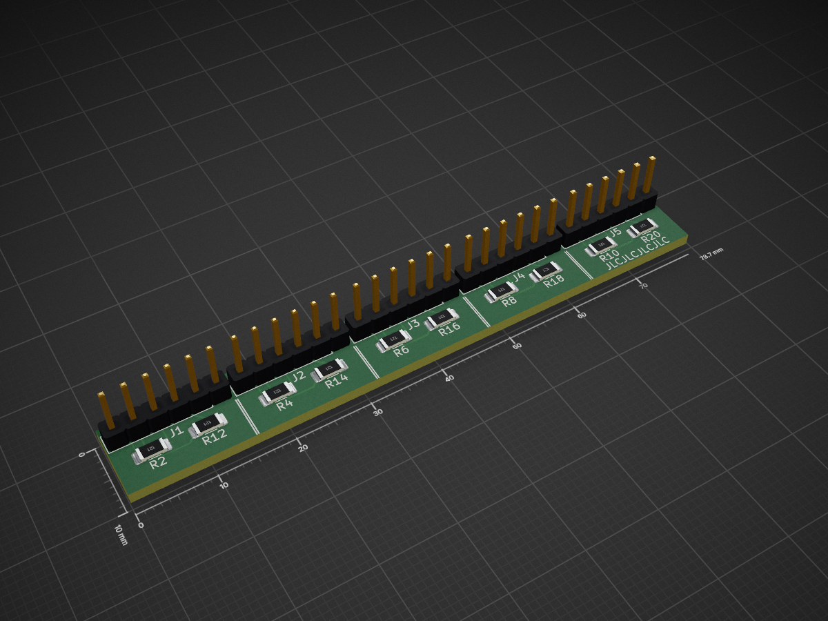
Hx711 is an open-source printed circuit board by tom01h, from the tom01h/Arduino-BendingSensor repository on GitHub. It is a 2-layer board of 78.7 × 10 mm with 25 parts on 30 nets, routed with 98 tracks and 0 vias.
Its parts include 20 resistors and 5 connectors.
Arduino UNO R4もどきのボードと自作基板を使って実験します
事情あって、センサー部分は実際にスキー場で使っているものですが、制御部分はスキー場で使っているものとは別のものです
センサー部分はひずみゲージ(BX120-100AA)とHX711(Mini Board)をちょい変(3.3V化)したものを使います
制御にはArduino UNO R4もどきのボードと自作基板を使います
D5端子がクロック、D2,D3,D4端子がデータ入力端子です
プログラムはBendingSensor.inoです
LCDに計測値を表示するためにu8g2ライブラリを使います
1秒に10回計測値を表示、最初の10回はゼロキャリブレーションに使います
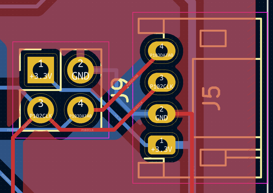
下の絵ではJ5,J9がDATA0(D4)で、絵には無いけどJ10,J11がDATA1(D3)でJ15,J16がDATA2(D2)です
それぞれ、どちらか一方のコネクタを使います
3.3Vに対応するためにここの真似をして改造します
(合成抵抗違うくね?って気はしますが…)
とっても細かい作業です
2個のひずみゲージと組み合わせてホイートストンブリッジを作るための基板がhx711.kicad_XXです
切り取って使います
0.8mm厚で作りました
あまり良くないと言われている基板同士のはんだ付け
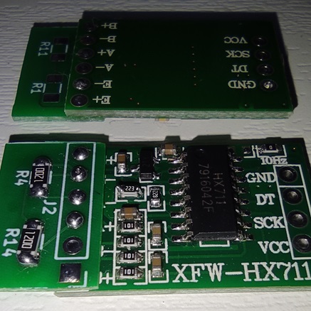
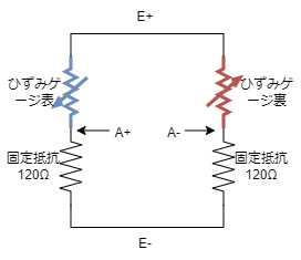
(E+)-(A+)間にひずみゲージを表向きに、(E+)-(A-)間にひずみゲージを裏向きに、(A+)-(E-)と(A-)-(E-)間は固定の抵抗(120Ω)をつなぎます
2枚使っているのは温度補償のため
スキー板の表裏に貼るわけにもいかないので、間に挟んだ0.4mm厚のプラバンに瞬間接着剤で固定しています
それ以外の部分は大体でついていればよいので両面テープで固定しています
断面図
センサー部分は上から
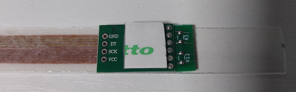
HX711をプラバンに止めているのは1.2mm厚の両面テープ

センサー部分の平面図

古い写真です
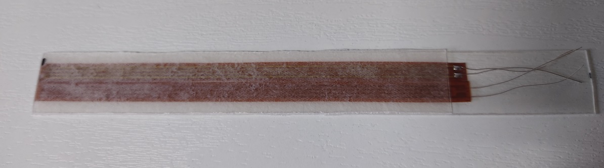
下の写真はHX711基板は裏返った状態
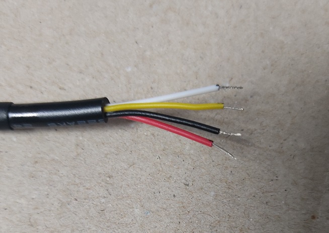
4芯のケーブルはこれのAWG28 4Coreを使っているのだけど、ちょっと固すぎな気がします
センサー(HX711)側は外皮(黒いの)2㎝だけむいて、中の線は5mmだけむいています
外皮をむくのにはこれを使っています
制御基板側は長めに外皮(黒いの)をむいて、熱収縮チューブで保護しています
コネクタはこれの4P
Groveコネクタっぽい見た目ですが、電源とGNDを逆にするという致命的な間違いをしています。今更直せないのでこのままいきますが…
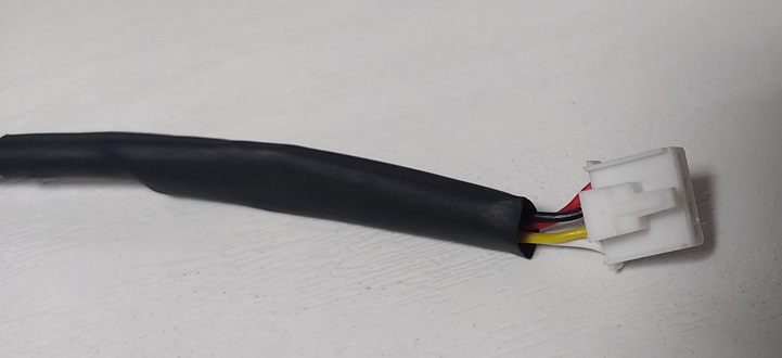
1枚目が表から見た絵で2枚目が裏から見た絵
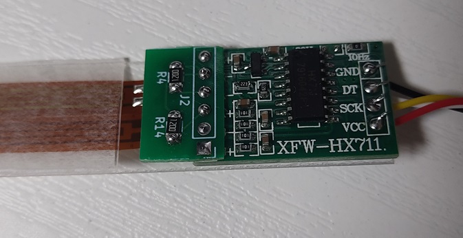
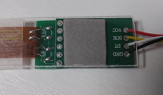
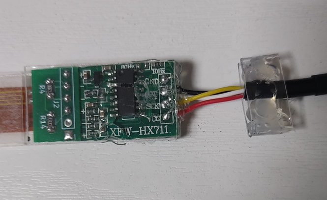
長さ16㎝に切った直径12mmの熱収縮チューブ12mmを全体の保護に使います
アイロンで加熱しますが、加熱しすぎに注意!!
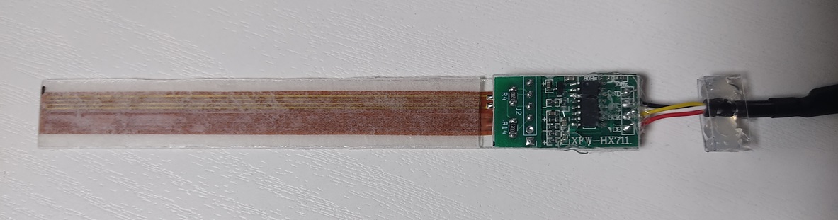
↑をチューブでくるむと↓になる
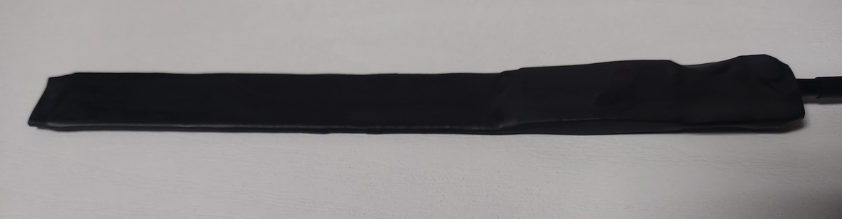
実際にスキー場で使うとノイズとドリフトがひどいのでバンドパスフィルターで後処理します
後処理でドリフト消すなら温度補償いらなかったのでは?とも思いますが…
import numpy as np
from scipy import signal
from scipy import stats

略

    #バターワースフィルタ(バンドパス)
    def bandpass(x, samplerate, fp, fs, gpass, gstop):
        fn = samplerate / 2                               #ナイキスト周波数
        wp = fp / fn                                      #ナイキスト周波数で通過域端周波数を正規化
        ws = fs / fn                                      #ナイキスト周波数で阻止域端周波数を正規化
        N, Wn = signal.buttord(wp, ws, gpass, gstop)      #オーダーとバターワースの正規化周波数を計算
        b, a = signal.butter(N, Wn, "band")               #フィルタ伝達関数の分子と分母を計算
        y = signal.filtfilt(b, a, x)                      #信号に対してフィルタをかける
        return y


略

    samplerate = 10
    gpass = 3    #通過域端最大損失[dB]
    gstop = 40   #阻止域端最小損失[dB]

# バンドパス| Qty | Value | Footprint | References |
|---|---|---|---|
| 20 | 120 | Resistor_SMD:R_1206_3216Metric_Pad1.30x1.75mm_HandSolder | R1, R2, R3, R4, R5, R10, R11, R12, R13, R14, R15, R16, R17, R18, R19, R20 +4 |
| 5 | gage | My:PinHeader_1x06_P2.54mm_Vertical | J1, J2, J3, J4, J5 |
google/mozc-devices
Circuit diagrams and firmware source code for Gboard DIY keyboards

davidphilipbarr/Sweep
Sweep - a small promicro based keyboard inspired by the Ferris.


hackclub/OnBoard
💡 Join 1,000 teenagers and make your first PCB with a $100 grant!

xyphro/UsbGpib
Versatile, cheap and portable USB to GPIB converter (USBTMC class based)


jes/scamp-cpu
A homebrew 16-bit CPU with a homebrew Unix-like-ish operating system.

It measures 78.7 × 10 mm and has 2 copper layers, 1.6 mm thick.
25 parts. The full list of its parts is on this page, with links to each part's symbol and footprint where PCBKit's library has them.
From the tom01h/Arduino-BendingSensor repository on GitHub, at the commit this page was made from: the board is hx711.kicad_pcb and its schematic hx711.kicad_sch. PCBKit opens the board in the browser, with nothing to install.
Its repository states no licence, so its author keeps all rights: ask tom01h before reusing the design.