

2 layers60 × 50 mm
Discrete PLL
adasbl/Discrete-PLL-pcb
Discrete PLL (Phase-Locked Loop) design implemented in KiCad
59 parts

 TofTo23/pll_pcb
Custom PCB for PLL (phase-locked loop)
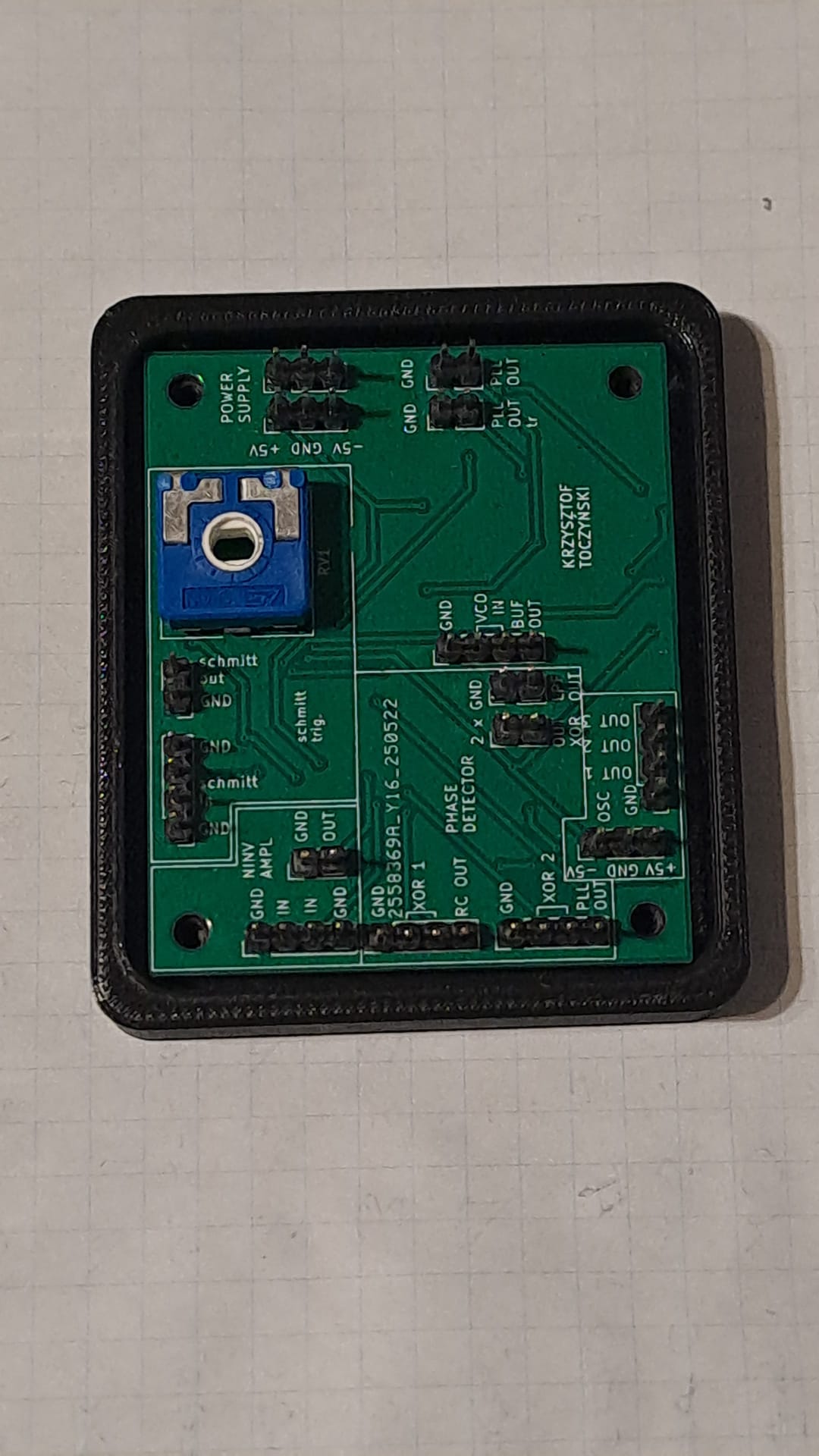
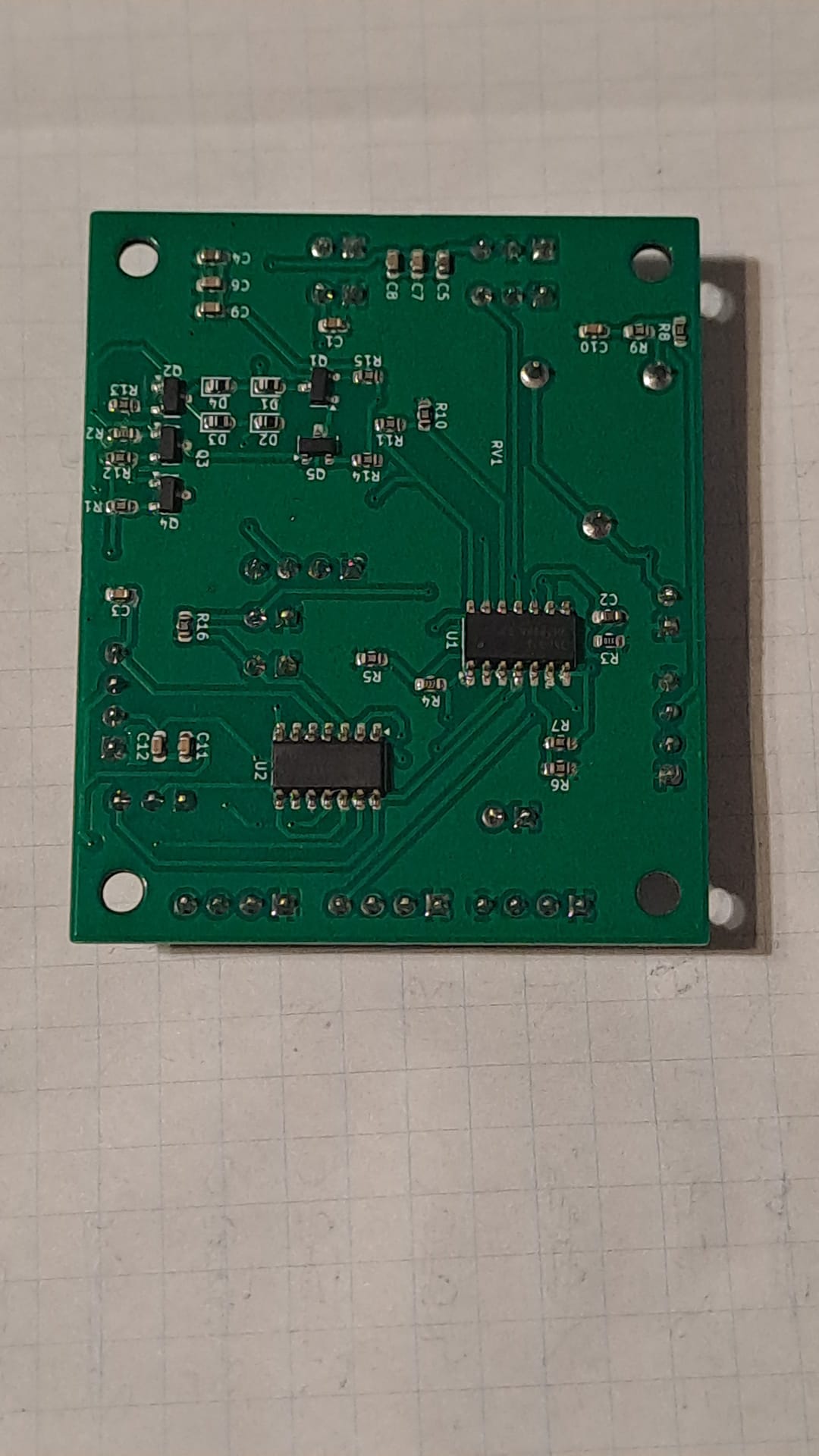
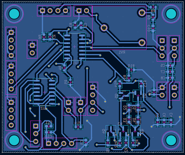
Pll chip is an open-source printed circuit board by TofTo23, from the TofTo23/pll_pcb repository on GitHub. It is a 2-layer board of 60 × 50 mm with 59 parts on 34 nets, routed with 392 tracks and 39 vias.
It is built around the CD4148WTP, BC846 and BC857. Its parts include 16 resistors, 15 connectors, 12 capacitors, 5 transistors and 4 diodes.
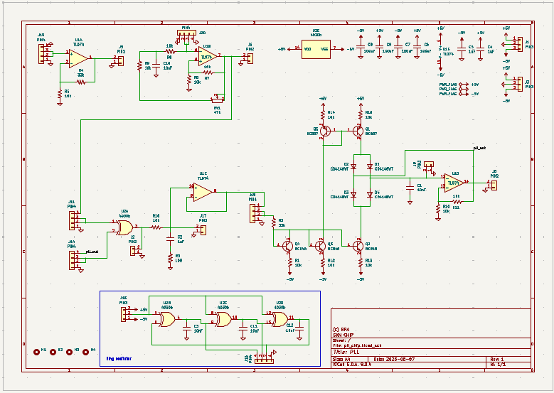
This repository covers designing the PLL schematic (LTSpice), creating the PCB layout, soldering and testing. Furthermore, there is the simple 3D model of case printed using 3D printer.
| Qty | Value | Footprint | References |
|---|---|---|---|
| 13 | 10k | Resistor_SMD:R_0603_1608Metric | R1, R5, R6, R7, R8, R9, R10, R11, R12, R13, R14, R15, R16 |
| 6 | PIN2 | Connector_PinHeader_2.54mm:PinHeader_1x02_P2.54mm_Vertical | J2, J5, J6, J8, J9, J17 |
| 6 | PIN4 | Connector_PinHeader_2.54mm:PinHeader_1x04_P2.54mm_Vertical | J11, J14, J16, J18, J19, J20 |
| 5 | 10nF | Capacitor_SMD:C_0603_1608Metric | C1, C3, C10, C11, C12 |
| 4 | 100nF | Capacitor_SMD:C_0603_1608Metric | C6, C7, C8, C9 |
| 4 | CD4148WT | Diode_SMD:D_0603_1608Metric | D1, D2, D3, D4 |
| 4 | MountingHole | MountingHole:MountingHole_3.2mm_M3_DIN965 | H1, H2, H3, H4 |
| 3 | 1uF | Capacitor_SMD:C_0603_1608Metric | C2, C4, C5 |
| 3 | BC846 | Package_TO_SOT_SMD:SOT-23 | Q2, Q3, Q4 |
| 3 | PIN3 | Connector_PinHeader_2.54mm:PinHeader_1x03_P2.54mm_Vertical | J1, J3, J15 |
| 2 | 33k | Resistor_SMD:R_0603_1608Metric | R2, R4 |
| 2 | BC857 | Package_TO_SOT_SMD:SOT-23 | Q1, Q5 |
| 1 | 10R | Resistor_SMD:R_0603_1608Metric | R3 |
| 1 | 4030b | Package_SO:SOIC-14_3.9x8.7mm_P1.27mm | U2 |
| 1 | 47k | potent:CA14 VA12,5 | RV1 |
| 1 | TL074 | Package_SO:SOIC-14_3.9x8.7mm_P1.27mm | U1 |
It measures 60 × 50 mm and has 2 copper layers, 1.6 mm thick.
59 parts, built around the CD4148WTP, BC846 and BC857. The full list of its parts is on this page, with links to each part's symbol and footprint where PCBKit's library has them.
From the TofTo23/pll_pcb repository on GitHub, at the commit this page was made from: the board is pll_chip.kicad_pcb and its schematic pll_chip.kicad_sch. PCBKit opens the board in the browser, with nothing to install.
Its repository states no licence, so its author keeps all rights: ask TofTo23 before reusing the design.
adasbl/Discrete-PLL-pcb
Discrete PLL (Phase-Locked Loop) design implemented in KiCad


juamonsan/ISCAS25_PCB
PCB that also serves as a pen holder in conmemoration of ISCAS 2025

SP8EBC/ParaPRZEKAZNIK-pcb
SPDT relays board controled by single TTL input, with an option for Modbus-RTU MCU module, with PT1000 temperature measurement


mgkoenig/lyft
LYFT is a sophisticated remote control for your IKEA BEKANT desk.