2 layers116.8 × 30 mm
Type d
google/mozc-devices
Circuit diagrams and firmware source code for Gboard DIY keyboards
14 parts3kApache-2.0
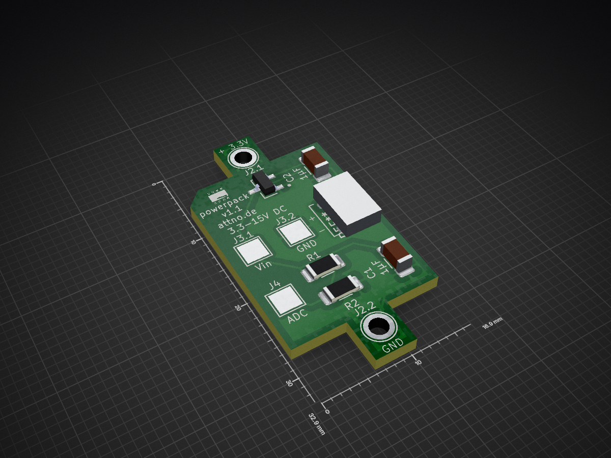
 theArcher73/attnode-powerpack3
AddOn to use the attnode v2/v3 with 3.3-15V DC
Powerpack is an open-source printed circuit board by theArcher73, from the theArcher73/attnode-powerpack repository on GitHub, published under the GPL-3.0 licence. It is a 2-layer board of 16.9 × 32.9 mm with 14 parts on 4 nets, routed with 40 tracks and 0 vias.
Its parts include 6 connectors, 2 capacitors, 2 resistors and 1 IC.
AddOn to use the attnode v2/v3 with 3.3-15V DC
This small pcb allows to run the attnode with an operating voltage between 3.3 and 15V, for example with a USB power supply, a LiPo or any other fixed voltage power supply.
It has the shape of the CR2032 battery clip and is soldered directly onto the attnode instead of the CR2032-Clip.
Therefore, when ordering the pcb's, a smaller pcb thickness can be used if possible, I have had good experiences with 1.2mm.
The power supply can be either via the JST socket, or the two pads directly on the pcb. In this case, the JST socket must not be soldered.
The voltage source must provide at least 120 mA.
Update 26.05.2021: add a Voltage divider added to monitor the Vin with an ADC pin of the ATTiny. The resistance ratio must be determined based on Vin, here are some sample values. The voltage at the ADC pad should not exceed 2.1V.
| Vin | Vmax | R1 | R2 |
|---|---|---|---|
| 3.7V | 4.2V | 1M | 1M |
| USB | 5.25V | 1M5 | 1M |
| 9V | 11V | 6M8 | 1M5 |
| 12V | 15.4V | 10M | 1M5 |
Attention! Pay attention to the peak voltage, which is higher than the nominal voltage for many batteries!
More information can be found here.
| front | back |
|---|---|
 |  |
The documentation of the attno.de-powerpack is distributed in the hope that it will be useful, but WITHOUT ANY WARRANTY; without even the implied warranty of MERCHANTABILITY or FITNESS FOR A PARTICULAR PURPOSE.
| Qty | Value | Footprint | References |
|---|---|---|---|
| 2 | 1µF | Capacitor_SMD:C_1206_3216Metric_Pad1.33x1.80mm_HandSolder | C1, C2 |
| 2 | R | Resistor_SMD:R_1206_3216Metric_Pad1.30x1.75mm_HandSolder | R1, R2 |
| 1 | ADC | TestPoint:TestPoint_Pad_2.5x2.5mm | J4 |
| 1 | GND | TestPoint:TestPoint_Pad_2.5x2.5mm | J3.2 |
| 1 | LOGO | logo:attnode_logo_sml_silk | G*** |
| 1 | MCP1703T-3302E_CB | MCP1703T-3302E_CB:SOT95P255X145-3N | U1 |
| 1 | Power_in 3.3-15V | Connector_JST:JST_SHL_SM02B-SHLS-TF_1x02-1MP_P1.00mm_Horizontal | J1 |
| 1 | Vin | TestPoint:TestPoint_Pad_2.5x2.5mm | J3.1 |
| 1 | Vout +3.3V | TestPoint:TestPoint_Plated_Hole_D2.0mm | J2.1 |
| 1 | Vout GND | TestPoint:TestPoint_Plated_Hole_D2.0mm | J2.2 |
The 12 most common of 14 parts.
It measures 16.9 × 32.9 mm and has 2 copper layers, 1.6 mm thick.
14 parts. The full list of its parts is on this page, with links to each part's symbol and footprint where PCBKit's library has them.
From the theArcher73/attnode-powerpack repository on GitHub, at the commit this page was made from: the board is kicad-project/powerpack.kicad_pcb. PCBKit opens the board in the browser, with nothing to install.
Its repository publishes it under the GPL-3.0 licence: you may reuse it on that licence's terms (keep the author's notice, and for a copyleft licence share your changes alike).
google/mozc-devices
Circuit diagrams and firmware source code for Gboard DIY keyboards


hackclub/OnBoard
💡 Join 1,000 teenagers and make your first PCB with a $100 grant!


Twotoz/C5VRX
Ultra-minimal, zero-CPU 5.8 GHz analog FPV video receiver using ESP32-C5 Wi-Fi 6 PHY MODEM_DIAG, BitScrambler WBFM demodulation & resistor DAC CVBS

