This repository contains the software and architecture for old Krone SplitFlap Displays. It works by using an ESP32 as a Master and then daisychains all modules using a daughter board for each element.
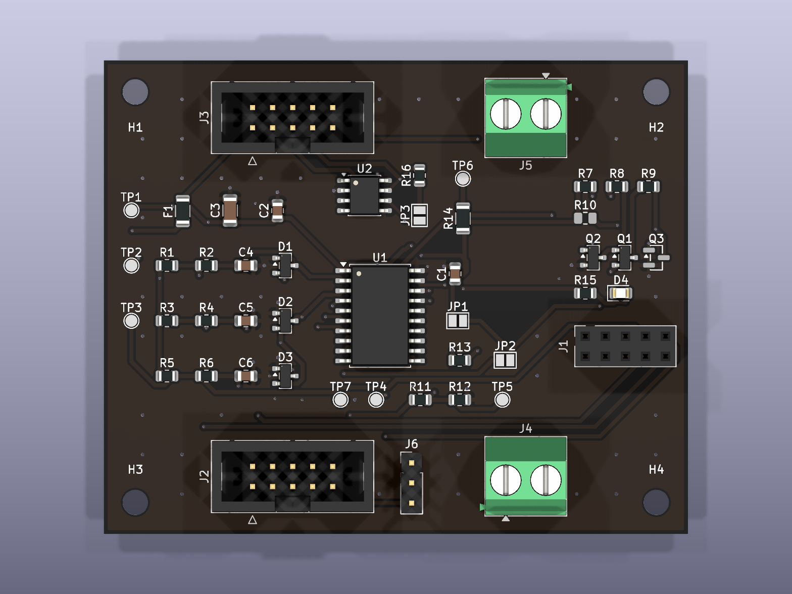
Master is an open-source printed circuit board by TenOfNine, from the TenOfNine/SmartKroneSplitFlap repository on GitHub. It is a 2-layer board of 68 × 54 mm with 37 parts on 26 nets, routed with 343 tracks and 112 vias.
It is built around the 74LVC1G17Z, TP8485E-SR and AO3401A, with the SM712 among its other parts. Its parts include 8 resistors, 5 capacitors, 4 connectors, 3 ICs and 2 diodes. It belongs with the ESP32 and RISC-V boards of this library.
KiCad-Projekt der Modulsteuerung (eine je Anzeigenmodul).
Stand: geroutet (2 Lagen, DRC 0 Fehler), Fertigungspaket committet unter
manufacturing/, bei JLCPCB in Auftrag.
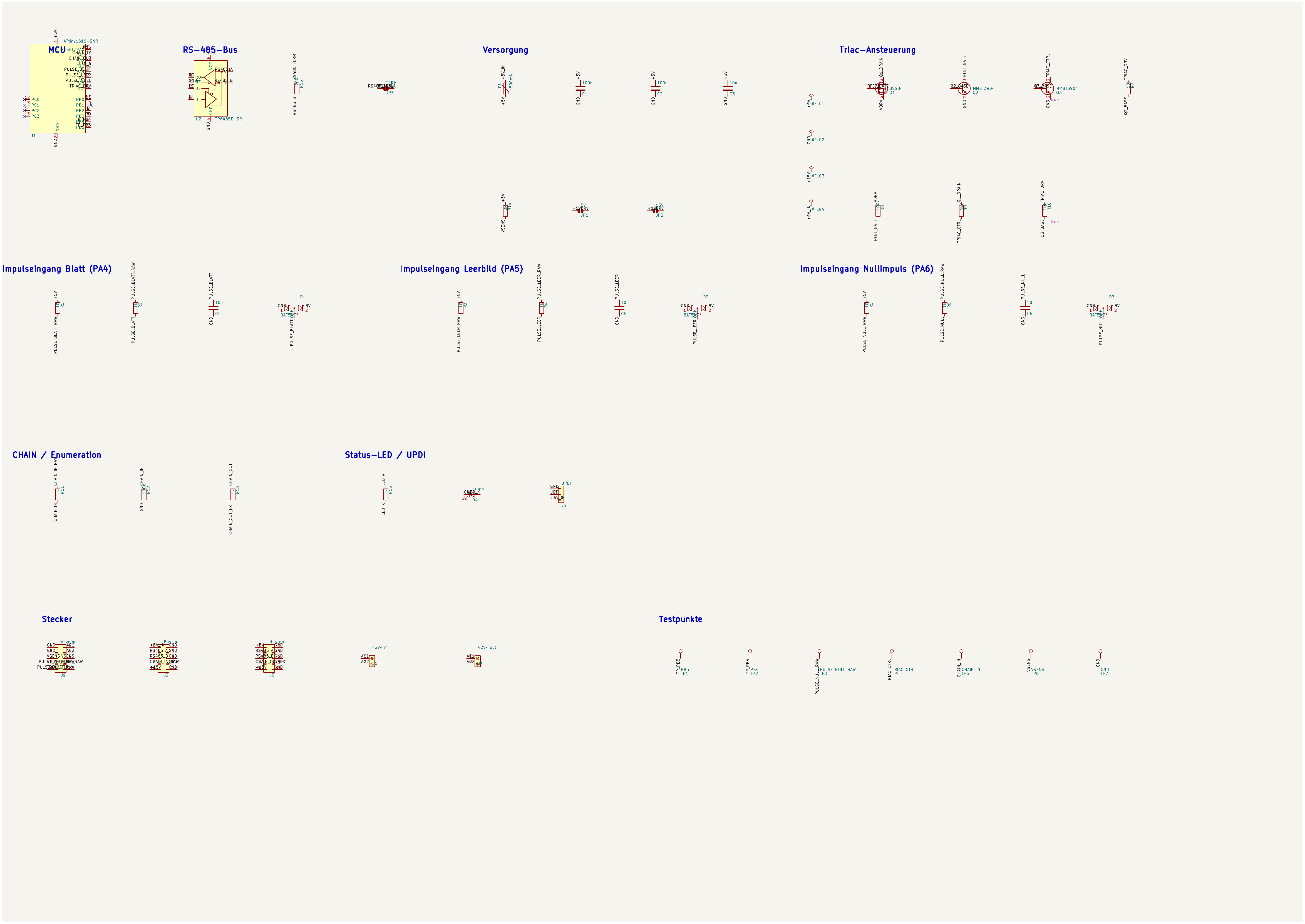
Vollauflösung Schaltplan: docs/daughtercard.pdf ·
ERC: 0 Fehler / 0 Warnungen (gen_daughtercard_sch.py --erc, in der CI geprüft)
Dateien
Datei
Herkunft
symbols/krone.kicad_sym
generiert von tools/build_krone_symbols.py aus der KiCad-9-Bibliothek. Alle 15 im Schaltplan verwendeten Symbole, abgeflacht. Nicht von Hand bearbeiten.
sym-lib-table
projektlokale Bibliothekstabelle, bindet krone über ${KIPRJMOD} ein
daughtercard.kicad_sch
generiert von tools/gen_daughtercard_sch.py aus Netzliste (docs/schaltplan-daughtercard.md Kap. 6) und Footprint-Tabelle (T5)
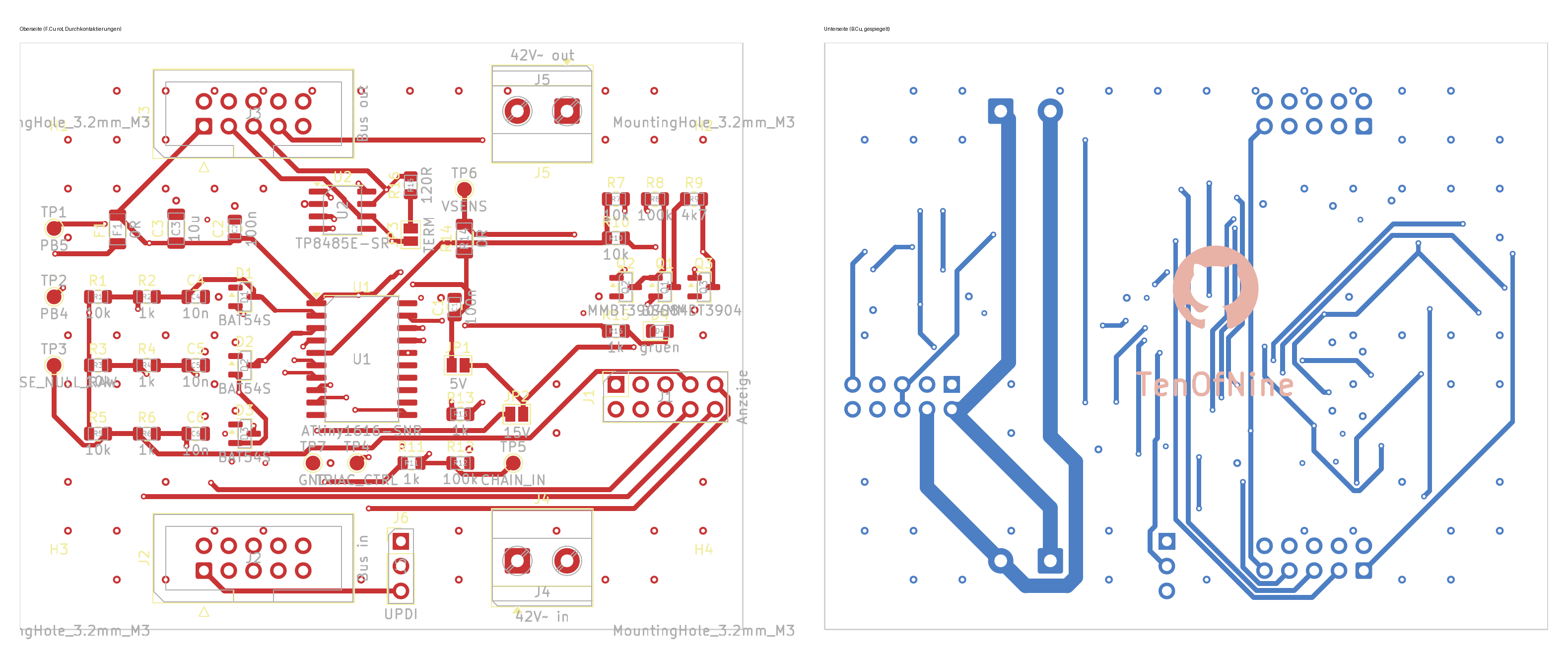
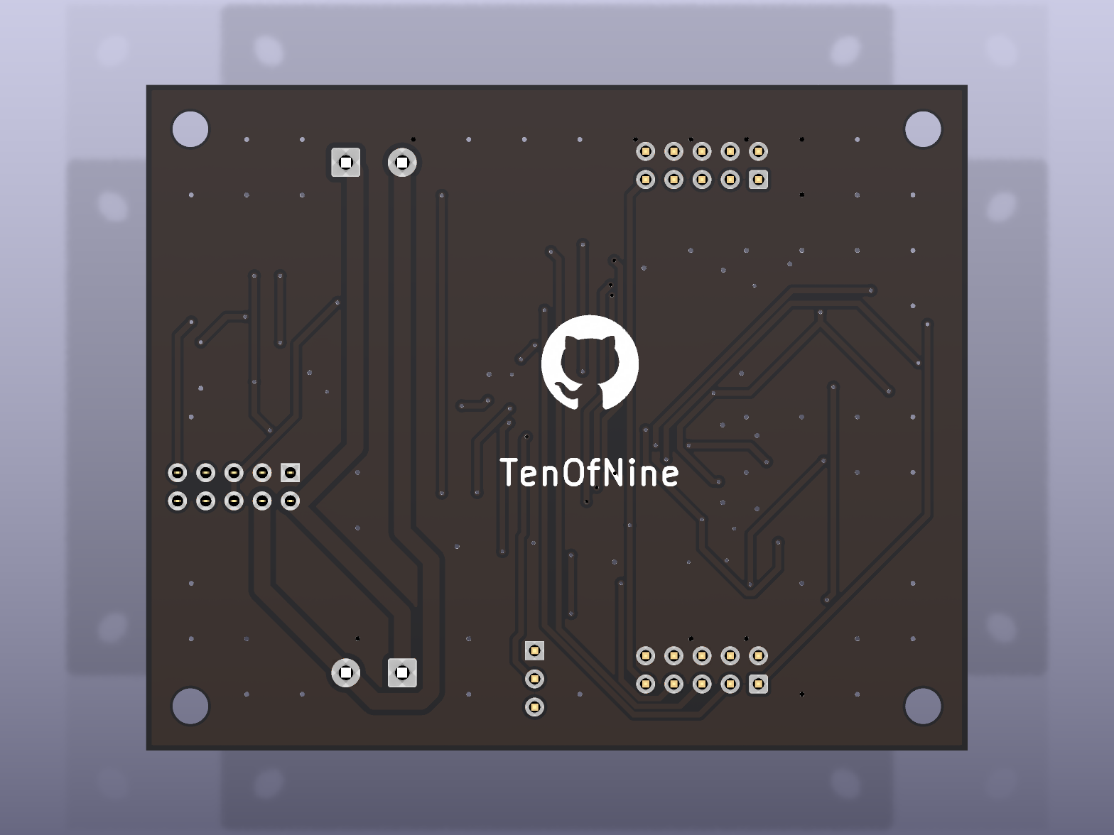
Erstplatzierung von tools/gen_daughtercard_pcb.py (System-Python, pcbnew), danach vom Betreiber feinjustiert und mit tools/route_daughtercard.py (FreeRouting + finish_routes.py + Masseflächen) verdrahtet. Maker-Mark / schwarz-weiß-Lagenaufbau von tools/add_silk_marks.py.
manufacturing/
committetes Fertigungspaket (Gerber, Bohrdatei, Zip, BOM, CPL, README) von tools/gen_manufacturing.py.
daughtercard.net
generiert (--netlist), nicht versioniert. PCB-Netzliste.
Neu erzeugen
bash
source .venv/bin/activate
python tools/build_krone_symbols.py                            # nur bei Änderung der Symbolauswahl
python tools/gen_daughtercard_sch.py --erc --pdf --png --netlist
Vorsicht bei der .kicad_pcb: Die Generatoren vergeben bei jedem Lauf neue
UUIDs. Solange die Platine noch nicht platziert/geroutet ist, gilt: .kicad_sch
.kicad_pcb nach einer Netzlistenänderung gemeinsam neu erzeugen und committen.
Sobald die .kicad_pcb platziert/geroutet ist (aktueller Stand), wird sie
nicht neu erzeugt — eine Netzlistenänderung erfordert stattdessen ein
UUID-Remapping der Footprint-Pfade (siehe Commit „F1 → 0-Ω-Brücke") und danach
tools/route_daughtercard.py. Details: docs/layout-daughtercard.md.
Flag
Ausgabe
--erc
docs/erc-daughtercard.rpt
--pdf
docs/daughtercard.pdf
--png
docs/daughtercard.png (Vorschau ohne Rahmen, für GitHub)
--netlist
daughtercard.net (PCB-Netzliste, nicht versioniert)
--check-only (bzw. --check bei build_krone_symbols.py) prüft ohne zu schreiben —
für die CI (T10). Der Check umfasst: jeder Pin an genau einem Netz oder NC, jedes
Bauteil mit vorhandenem Footprint.
Netznamen tragen im Netlist-Export das KiCad-übliche Wurzelblatt-Präfix (/+5V,
/GND …), weil die Rails über lokale Labels laufen. Für den PCB-Import ist das
unerheblich; wer es ohne Präfix will, stellt die Rails auf Power-Symbole um.
Zum Schaltplan
Die Verbindungen werden über gleichnamige lokale Labels an den Pins hergestellt,
nicht über gezeichnete Leitungen. Die Bauteile liegen in einem groben Raster, nicht
handverlegt. Das ist bewusst so:
Die menschenlesbare Darstellung der Schaltung ist docs/schaltplan-daughtercard.md
Kapitel 5 (Prinzipschaltbilder) und Kapitel 6 (verbindliche Netzliste).
Die .kicad_sch ist das maschinell erzeugte Abbild von Kapitel 6 für ERC,
Netzlistenexport und – nach dem Footprint-Schritt T5 – das Layout.
Eine handverlegte, ablesbare Schaltplanseite kann später folgen; sie ist nicht
Teil von T4.
Layout (T5) und Routing
Footprints sind allen 48 Bauteilen zugeordnet (FOOTPRINTS in
tools/gen_daughtercard_sch.py). Die Platine ist geroutet — Zonen, Netzklassen
(alle Bahnen 0,5 mm außer AC 1,5 mm), Masseflächen und die offenen Punkte mit
Layoutbezug stehen in docs/layout-daughtercard.md,
die JLCPCB-Bestückung in docs/jlc-bestueckung.md.
Prüfpunkte
Die zwei Netzlisten-Entscheidungen aus T4 (P-1 Testpads, P-2 BAT54S) sind vom
Betreiber freigegeben, siehe docs/pruefpunkte-t4.md.
It measures 68 × 54 mm and has 2 copper layers, 1.6 mm thick.
What parts does the Master use?
37 parts, built around the 74LVC1G17Z, TP8485E-SR, AO3401A and SM712. The full list of its parts is on this page, with links to each part's symbol and footprint where PCBKit's library has them.
Where can I download the Master KiCad files?
From the TenOfNine/SmartKroneSplitFlap repository on GitHub, at the commit this page was made from: the board is hardware/master/master.kicad_pcb and its schematic hardware/daughtercard/daughtercard.kicad_sch. PCBKit opens the board in the browser, with nothing to install.
Can I use the Master design in my own project?
Its repository states no licence, so its author keeps all rights: ask TenOfNine before reusing the design.
This repository contains the software and architecture for old Krone SplitFlap Displays. It works by using an ESP32 as a Master and then daisychains all modules using a daughter board for each element.
Open fieldeyesv2.kicadpro in KiCad 9. The whole circuit is one flat schematic (fieldeyesv2.kicadsch): all 168 parts are on a single page, in four framed sections.