
4 layers43.2 × 43.2 mm

 taroz/Smartphone-GNSS-Booster86
Smartphone GNSS Booster
Gnss booster is an open-source printed circuit board by taroz, from the taroz/Smartphone-GNSS-Booster repository on GitHub, published under the MIT licence. It is a 2-layer board of 50 × 57.5 mm with 19 parts on 10 nets, routed with 23 tracks and 447 vias.
It is built around the PD0922J5050S2HF, AXGD10402KR and FC0603E1000BTBST1, with the FCHP0402E50R0BGT1, GJM1555C1H470FB01D and HP5354.A among its other parts. Its parts include 5 resistors, 4 capacitors, 4 diodes, 2 ICs and 2 connectors. It belongs with the radio and wireless boards of this library.


Smartphone-mounted GNSS signal re-radiator, designed in KiCad 10.
An external active GNSS antenna (Harxon HX-CU7603A or Beitian BT-230F, with its own LNA, powered through the coax by this board) is connected to the SMA input. The board splits the signal into L1 and L5 paths and feeds a dual-band patch antenna on the back side, which re-radiates the signal into the smartphone's internal GNSS antenna. The phone therefore receives a much cleaner signal than it would with its own antenna alone, which is what makes RTK with the android-rtcm-streamer app practical.
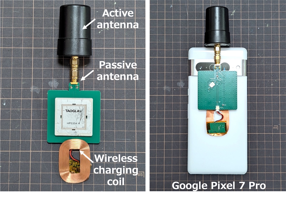
Off-the-shelf parts used together with the board:
J1.J2 and powers the board and, through the bias tee, the
active antenna's LNA.| Top (components) | Bottom (patch antenna) |
|---|---|
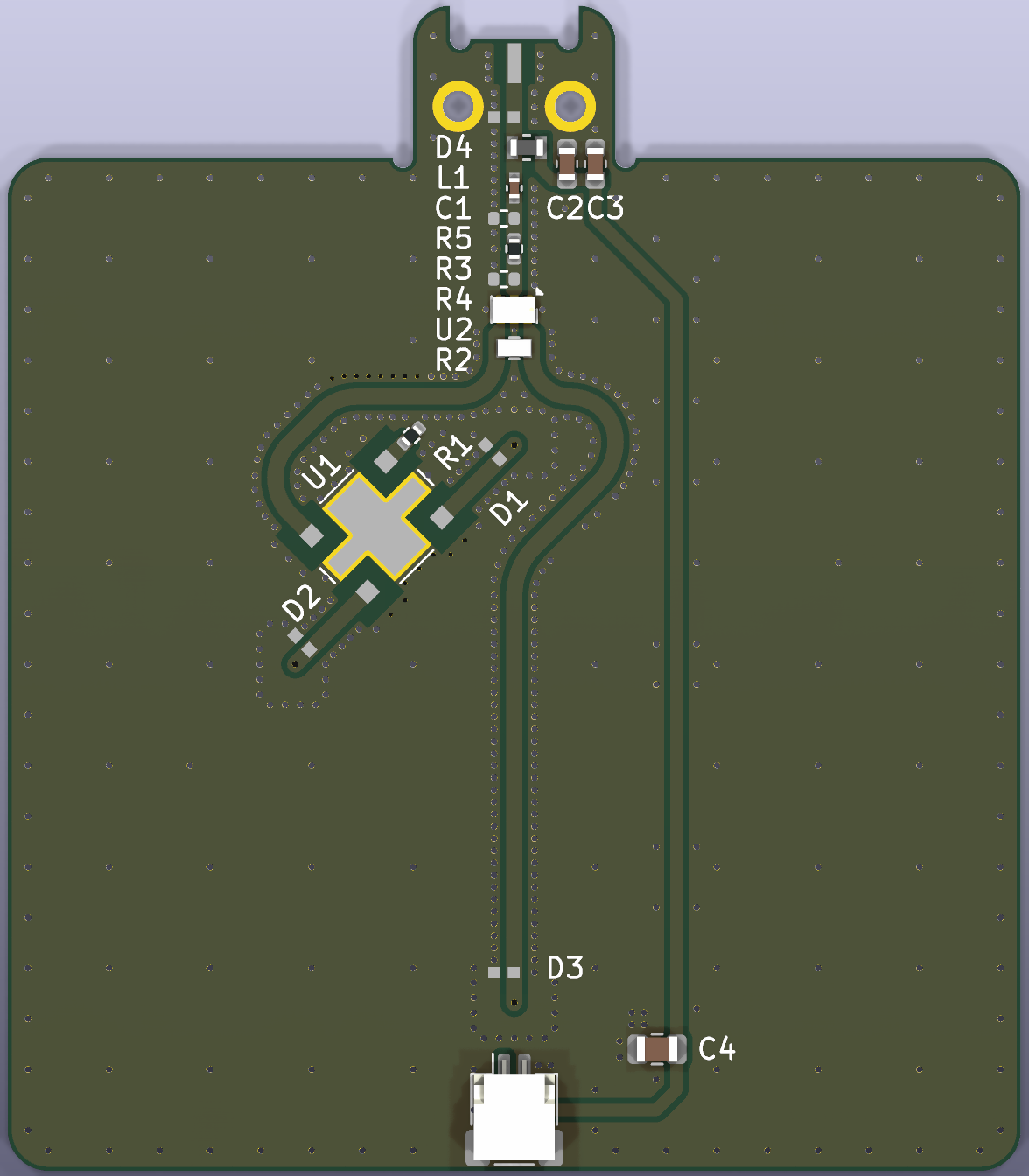 |  |
Signal path, from the SMA input J1 to the patch antenna AE1:
L1 (120 nH) injects +5 V from J2 onto the coax to
power the external antenna's LNA; C1 (47 pF) blocks the DC from the RF path.
C2/C3/C4 decouple the supply.R3/R4/R5 (37 Ω series, 150 Ω shunts) form a ~6 dB π attenuator
that sets the re-radiated level and improves the match seen by the divider.U2 (TTM Xinger PD0922J5050S2HF, 0.95–2.15 GHz Wilkinson)
splits the signal into an L1 and an L5 branch. R2 (100 Ω) is the divider's
isolation resistor.U1 (TTM Xinger X3C14P1-03S, 1.2–1.7 GHz 3 dB 90° hybrid) drives the
two orthogonal L1 feed points of the patch in quadrature to produce circular
polarization. R1 (50 Ω) terminates the hybrid's isolated port.D1–D4 (Littelfuse AXGD10402KR) on the SMA input and on each
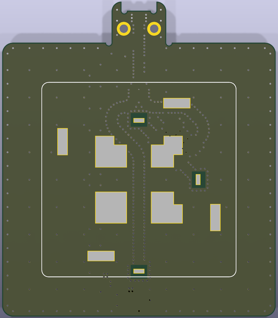
antenna feed.The patch antenna (Taoglas HP5354.A, 35 × 35 mm, L1 + L5) is mounted on the bottom side, so the top side with the components faces away from the phone.
| Item | Value |
|---|---|
| Size | 50 × 57.5 mm (50 × 50 mm body plus the SMA tab) |
| Layers | 2 (F.Cu / B.Cu), FR-4 core 0.71 mm, total 0.8 mm |
| Surface finish | ENIG |
| Min. track / clearance | 0.1 mm / 0.1 mm |
| Min. via | 0.41 mm diameter, 0.2 mm drill |
Fabrication and assembly files exported for JLCPCB with the Fabrication Toolkit
plugin are in production/:
gnss-booster.zip – Gerbers and drill filesbom.csv – BOM with LCSC part numbers (the R4/R5 150 Ω 0402 resistors have no
LCSC number; any 1 % 0402 part works)positions.csv – component placement (CPL)netlist.ipc – IPC-D-356 netlistdesignators.csv – reference designators| Ref | Part | Package | Function | LCSC |
|---|---|---|---|---|
| AE1 | Taoglas HP5354.A | 35 × 35 mm patch | L1/L5 re-radiating patch antenna (bottom side) | C30042276 |
| U1 | TTM Xinger X3C14P1-03S-1 | 6.35 × 5.08 mm | 3 dB 90° hybrid coupler, L1 quadrature feed | C36369905 |
| U2 | TTM Xinger PD0922J5050S2HF | 0805 (6-pad) | Wilkinson power divider, L1/L5 split | C5136968 |
| R1 | Vishay FCHP0402E50R0BGT1, 50 Ω | 0402 | Hybrid isolated-port termination | C4267592 |
| R2 | Vishay FC0603E1000BTBST1, 100 Ω | 0603 | Divider isolation resistor | C2076508 |
| R3 | 37 Ω | 0402 | π attenuator, series | C17168 |
| R4, R5 | 150 Ω | 0402 | π attenuator, shunt | – |
| C1 | Murata GJM1555C1H470FB01D, 47 pF | 0402 | DC block | C882562 |
| C2 | 0.1 µF | 0603 | Supply decoupling | C14663 |
| C3 | 1 µF | 0603 | Supply decoupling | C15849 |
| C4 | 10 µF | 0805 | Supply decoupling | C440198 |
| L1 | Murata LQW18ANR12G80D, 120 nH | 0603 | Bias-tee inductor | C307612 |
| D1–D4 | Littelfuse AXGD10402KR | 0402 | ESD protection | C434715 |
| J1 | Molex 73251-2440 | SMA female, edge mount | RF input from the external antenna | C588468 |
| J2 | JST SM02B-SRSS-TB | SH 1.0 mm, 2 pin | +5 V power input | C160402 |
Open gnss-booster.kicad_pro in KiCad 10 (or newer). The project is self-contained:
libs/gnss-booster.kicad_sym and
libs/gnss-booster.pretty, referenced through the
project-local sym-lib-table / fp-lib-table as library gnss-booster.libs/3d/. STEP files are
included for the Xinger power divider and the Vishay 0603 resistor; the models for the
patch antenna, the hybrid coupler and the SMA connector are vendor files that are not
redistributed here. Missing models only affect the 3D viewer.This board re-radiates GNSS signals. Depending on your country, operating a GNSS re-radiator may require a license or may be restricted to shielded environments. Check your local radio regulations before use.
Copyright (c) 2026 Taro Suzuki.
This hardware design (schematic, layout, libraries, fabrication outputs and this
documentation) is licensed under the CERN Open Hardware Licence Version 2 - Permissive
(CERN-OHL-P-2.0). You may redistribute and modify it under the terms of that licence,
see LICENSE or https://ohwr.org/cern_ohl_p_v2.txt. It is distributed
WITHOUT ANY EXPRESS OR IMPLIED WARRANTY, including of merchantability, satisfactory
quality and fitness for a particular purpose.
The Android app in android-rtcm-streamer/ is licensed
separately under the MIT License (see the repository root LICENSE).
Component datasheets and 3D models are the property of their respective manufacturers.
Takuho Munetomo contributed to the design of this board.
| Qty | Value | Footprint | References |
|---|---|---|---|
| 4 | AXGD10402KR | gnss-booster:D_Littelfuse_AXGD10402KR_0402_1005Metric_1.02x0.51mm | D1, D2, D3, D4 |
| 2 | 150 | Resistor_SMD:R_0402_1005Metric | R4, R5 |
| 1 | 0.1u | Capacitor_SMD:C_0603_1608Metric | C2 |
| 1 | 10u | Capacitor_SMD:C_0805_2012Metric | C4 |
| 1 | 1u | Capacitor_SMD:C_0603_1608Metric | C3 |
| 1 | 37 | Resistor_SMD:R_0402_1005Metric | R3 |
| 1 | Conn_01x02_MountingPin | Connector_JST:JST_SH_SM02B-SRSS-TB_1x02-1MP_P1.00mm_Horizontal | J2 |
| 1 | Conn_Coaxial | gnss-booster:SMA_Molex_732512440_Female_Embed | J1 |
| 1 | FC0603E1000BTBST1 | gnss-booster:R_Vishay_FC0603xxxxxxTxx_0603_1608Metric_1.626x0.813mm | R2 |
| 1 | FCHP0402E50R0BGT1 | Resistor_SMD:R_0402_1005Metric | R1 |
| 1 | GJM1555C1H470FB01D | gnss-booster:C_Murata_xxx15_0402_1005Metric_1.0x0.5mm | C1 |
| 1 | HP5354.A | gnss-booster:Taoglas_HP5354.A_GNSS | AE1 |
| 1 | LQW18ANR12G80D | gnss-booster:L_Murata_LQW18ANxxxx80x_0603_1608Metric_1.65x0.99mm | L1 |
| 1 | PD0922J5050S2HF | gnss-booster:Xinger_0805_2012Metric-6_Pad0.33x0.41mm | U2 |
| 1 | X3C14P1-03S-1 | gnss-booster:RF_HybridCoupler_TTM_X3C14P1-03S | U1 |

takuhoTech/CelestNavi-Fusion
Ready-to-use GNSS+CLAS receiver with integrated patch antenna

takuhoTech/CelestNavi-Combo
Ready-to-use GNSS+CLAS receiver with integrated loop antenna

TUDSSL/FreeBie
To compile FreeBie runtime we used the GNU Arm Embedded Toolchain (9.3.1) and CMake (3.19.1) to build the project. To program the MCU we used the J-Link debug probe with the accompanying J-Link software.

Brazil-L/Lumeward-OpenSource
Open-source Lumeward firmware and development tools


osqzss/PocketSDR
The Pocket SDR FE device includes 2, 4, or 8 RF frontend channels, supporting the GNSS L1 band (1525 - 1610 MHz) or L2/L5/L6 bands (1160 - 1290 MHz). For these signal bands, refer to GNSS Signal Bands.

antmicro/polarfire-som
System on Module based on Microchip PolarFire MPFS250T SoC
It measures 50 × 57.5 mm and has 2 copper layers, 0.8 mm thick.
19 parts, built around the PD0922J5050S2HF, AXGD10402KR, FC0603E1000BTBST1 and FCHP0402E50R0BGT1. The full list of its parts is on this page, with links to each part's symbol and footprint where PCBKit's library has them.
From the taroz/Smartphone-GNSS-Booster repository on GitHub, at the commit this page was made from: the board is gnss-booster/gnss-booster.kicad_pcb and its schematic gnss-booster/gnss-booster.kicad_sch. PCBKit opens the board in the browser, with nothing to install.
Its repository publishes it under the MIT licence: you may reuse it on that licence's terms (keep the author's notice, and for a copyleft licence share your changes alike).