2 layers

 sylefeb/skidl-tools6
A set of tool to interact with SKiDL and KiCad
Board3 edit is an open-source printed circuit board by sylefeb, from the sylefeb/skidl-tools repository on GitHub. It is a 2-layer board of 19.6 × 18 mm with 9 parts on 2 nets.
This tool helps doing iterative design between a PCB described in skidl (python code) and KiCad's PCB editor (PcbNew): start placing and routing, go back to code and add components, resume editing without loosing your previous changes.
Note: (thanks to TheZoq2 for pointing this out) In many cases you do not need this
tool and can simply use generate_netlist() from skidl and use KiCad's Import > Netlist
feature to merge changes with your current PCB design. Best to try that first as KiCad provides
multiple options in dealing with conflicts.
A collection of tools (one for now!) to help with PCB design using KiCad and skidl.
The main tool is skidl-updater, it takes a previous design and a newly generated
PCB from skidl, and remaps prior edits onto the new file. See Example workflow below.
This is very much work in progress, please see Limitations.
git submodule init
git submodule update
mkdir BUILD
cd BUILD
cmake ../updater/
make installThis tutorial example walks through the process of progressively adding components to a board, using skidl-updater at each step to import prior changes to the PCB. For the sake of the tutorial the example is voluntarily cut
into many small incremental steps.
Note: the tutorial assumes some familiarity with KiCad's layout editor (PcbNew).
This tutorial uses KiCad 7.
The goal is to design a simple 'half-PMOD' (using only one PMOD row)
with four LEDs on it. All files are in examples/pmod_leds.
Here is the workflow:
ref attribute (PMOD), this is essential to the inner workings of skidl-updater: each component has to have a unique ref.
To generate the board we run python board1.py.Note: the script has to be run from a special python environment provided by KiCad, please refer to skidl's documentation.
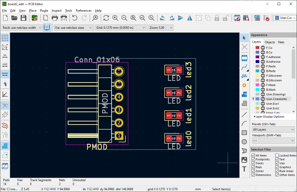
python board2.py.
However board2.kicad_pcb has lost the contour and placement of the connector we did at step one. We don't want to redo what we just did, so we use skidl-updater:skidl-updater -p board1.kicad_pcb -n board2.kicad_pcb -o board2_edit.kicad_pcb
board1.kicad_pcb as reference and imports it into board2.kicad_pcb to obtain board2_edit.kicad_pcb. We now can open board2_edit.kicad_pcb and are ready to place the LEDs, prior edits have been imported! We now place the LEDs neatly on the board, save and exit.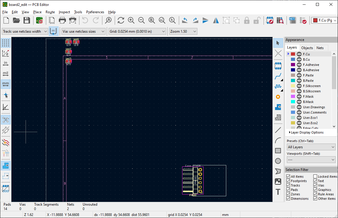
python board3.py to obtain board3.kicad_pcb, which has again lost all our edits. skidl-updater to the rescue!skidl-updater -p board2_edit.kicad_pcb -n board3.kicad_pcb -o board3_edit.kicad_pcb
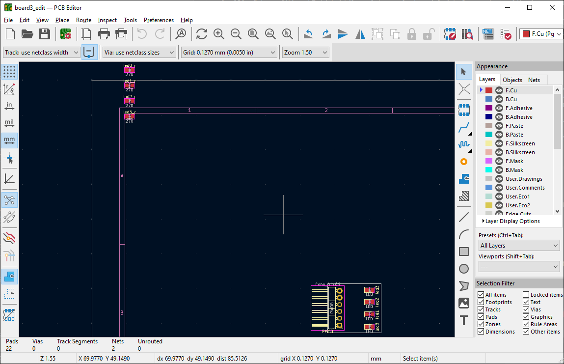
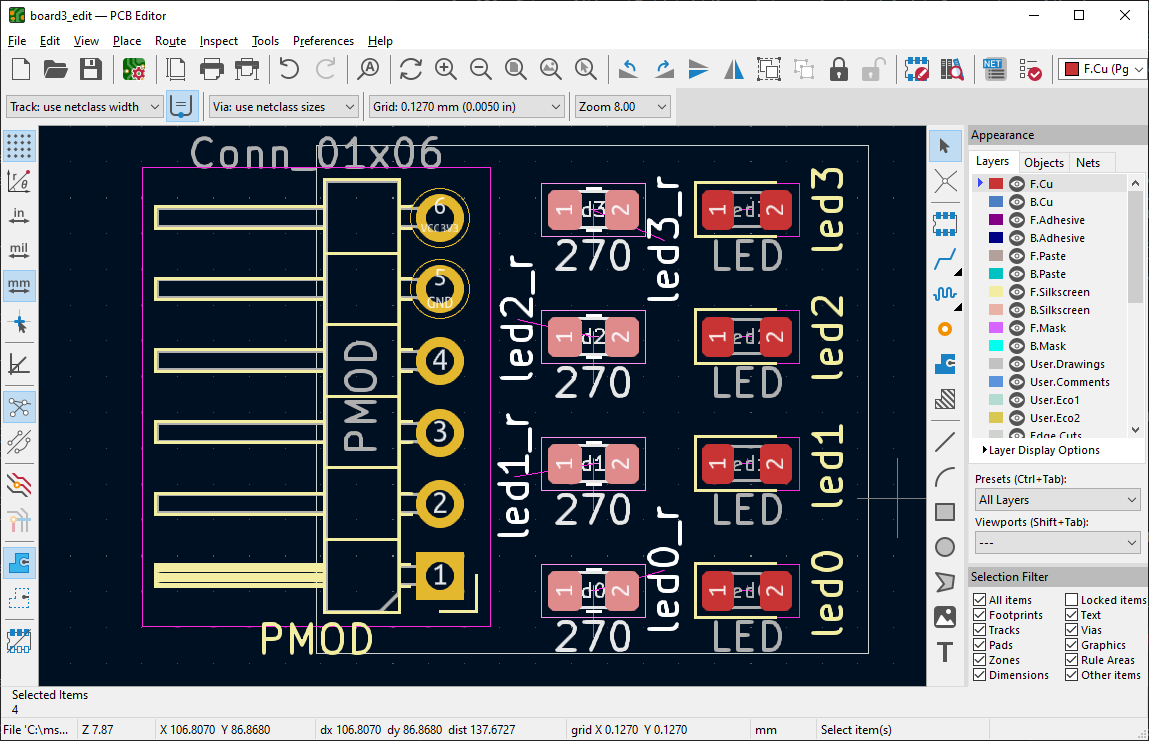
python board4.py. Again all changes are lost, and we use skidl-updater to save the day:skidl-updater -p board3_edit.kicad_pcb -n board4.kicad_pcb -o board4_edit.kicad_pcb
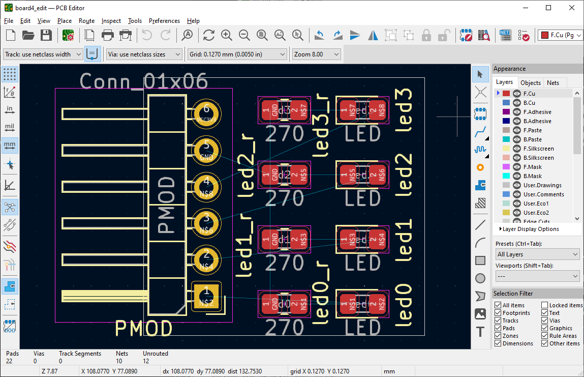
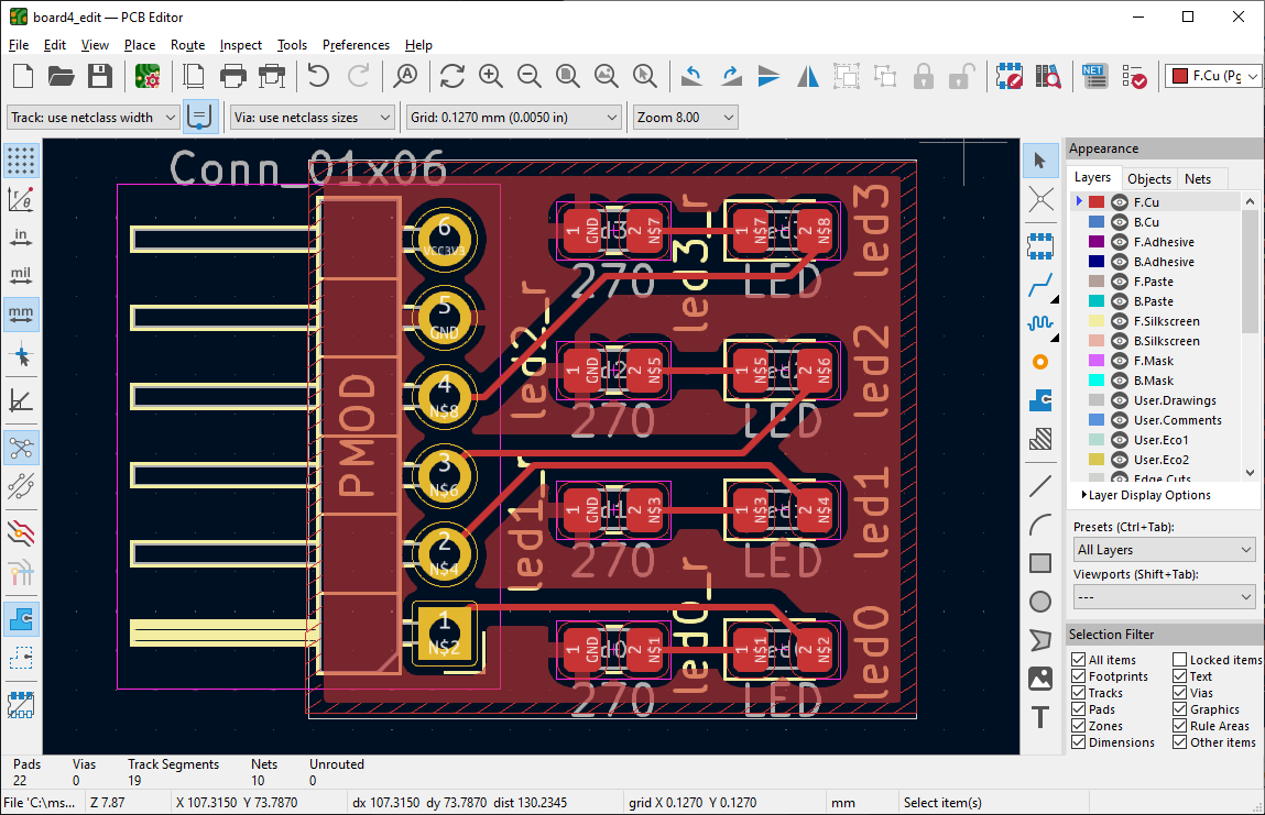
The board is done! (maybe don't fab it, it's just a quick example ;) ).
Note: In the example we save each step, but of course you can start from the same file, running
skidl-updater -p board_edit.kicad_pcb -n board.kicad_pcb -o board_edit.kicad_pcbworks (it will rename the previous file as a.bak, in case something goes wrong).
There are potential 'gotchas', be worried if kicad reports a warning when opening the PCB file.
Use at your own risks -- always double check your design and the nets.
Some known issues and workarounds:
Removing a component. The tool is geared towards the idea of progressively
adding components to the board. When removing a component, that is the script
no longer produce a component of a given ref, then edit the previous version
.kicad_pcb and also delete the component from the board. Otherwise, the
updater will keep bringing it back, introducing various problems with nets.
Swapping the footprint of a component. As with Removing a component,
make sure to edit the previous version .kicad_pcb and delete the component
first. You will have to place the new footprint again, but that guarantees the
footprint is properly updated.
Found another limitation? Please fill-in an issue in github.
| Qty | Value | Footprint | References |
|---|---|---|---|
| 4 | 270 | R_0805_2012Metric_Pad1.20x1.40mm_HandSolder | led0_r, led1_r, led2_r, led3_r |
| 4 | LED | LED_0805_2012Metric_Pad1.15x1.40mm_HandSolder | led0, led1, led2, led3 |
| 1 | Conn_01x06 | PinHeader_1x06_P2.54mm_Horizontal | PMOD |


FrameworkComputer/ExpansionCards
Reference designs and documentation to create Expansion Cards for the Framework Laptop

VoronDesign/Voron-Hardware
Cool Hardware designed by the Voron Design group

hackclub/OnBoard
💡 Join 1,000 teenagers and make your first PCB with a $100 grant!


adamws/kicad-kbplacer
KiCad plugin for automatic keyboard's key placement and routing
It measures 19.6 × 18 mm and has 2 copper layers, 1.6 mm thick.
9 parts. The full list of its parts is on this page, with links to each part's symbol and footprint where PCBKit's library has them.
From the sylefeb/skidl-tools repository on GitHub, at the commit this page was made from: the board is examples/pmod_leds/board3_edit.kicad_pcb. PCBKit opens the board in the browser, with nothing to install.
Its repository states no licence, so its author keeps all rights: ask sylefeb before reusing the design.