
2 layers290.1 × 130 mm
 SunritHazra/HackroDevX
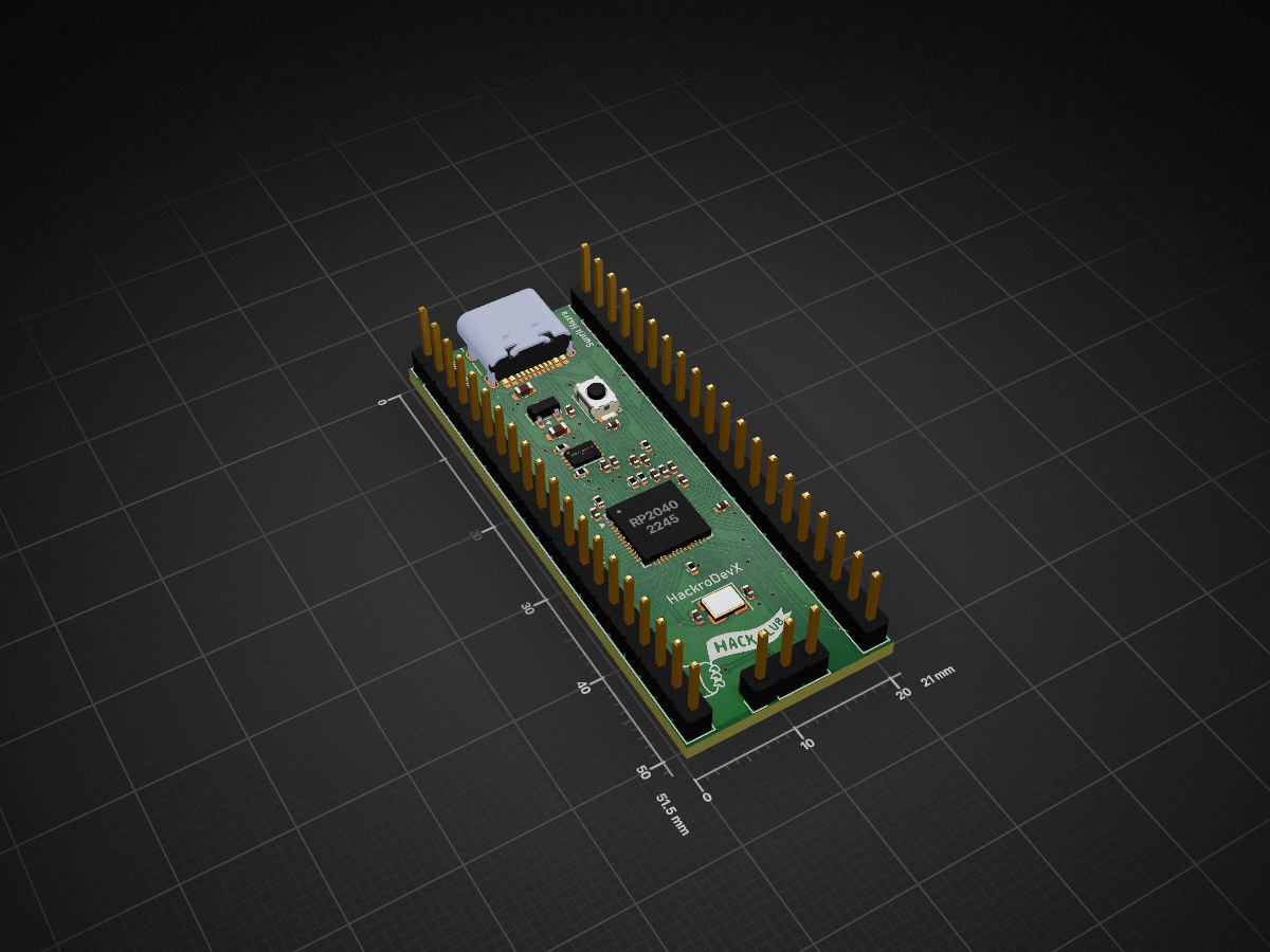
A development board (devboard) based on Raspberry Pi RP2040 SoC with USB-C connectivity.
HackroDevX is an open-source printed circuit board by SunritHazra, from the SunritHazra/HackroDevX repository on GitHub, published under the MIT licence. It is a 2-layer board of 21 × 51.5 mm with 34 parts on 55 nets, routed with 576 tracks and 68 vias.
It is built around the RP2040. Its parts include 17 capacitors, 7 resistors, 4 connectors, 3 ICs and 1 switch. It belongs with the microcontroller boards boards and the RP2040 boards of this library.
An open-source RP2040 development board with USB-C power/programming, onboard QSPI flash, and a Raspberry Pi Pico-compatible pinout. Built by following Hack Club's "Custom Devboard" starter project guide, entirely in KiCad. This is my first custom PCB from schematic to fabrication.
Full day-by-day design log, decisions, and mistakes: Engineering Log.md (see also JOURNAL.md and Fabrication Log.md)
Project stats: 5 build-log days · ~25h 00m total design time · 100% designing progress, 0% building progress (as of the latest journal entry — board is ordered for PCBA, not yet assembled)
On the name: Follows the author's personal naming convention for electronics projects — "Hackro" as the base word, a short form of the project's defining trait ("Dev", for devboard), and a single trailing letter — giving HackroDevX.
Full Schematic
The schematic follows the five functional blocks the guide breaks a devboard into: power/decoupling, USB-C, the crystal oscillator, QSPI flash storage, and the I/O breakout, all wired around a central RP2040.
Power & decoupling: One 0.1uF decoupling capacitor per RP2040 VDD pin — eight on the 3.3V IOVDD rail, two on the 1.1V DVDD rail — plus a 1uF bulk capacitor on each rail to smooth larger ripples. Power labels face up, ground labels face down, per standard schematic convention. This is the power and decopuling.
USB-C & step-down: A USB-C receptacle with SHIELD/GND tied to ground, CC1/CC2 pulled down through 5.1KΩ resistors so the port negotiates power delivery, and the D+/D- lines routed through 27Ω termination resistors into the RP2040's USB_DP/USB_DM pins (set to bidirectional global labels). VBUS is stepped down from 5V to 3.3V using an MCP1700x-330xxTT LDO (swapped in from the guide's larger NCP1117-3.3_SOT223 for a smaller footprint, at the cost of a lower 250mA current limit), with 10uF bulk capacitors bracketing it. This is the USB-C and step down.
Crystal oscillator: A 12MHz crystal (Y1) with two load capacitors on its I/O pins (bumped from the guide's 15pF to 33pF to match the load capacitance of the specific crystal part used), pins 2/4 tied to GND, and a 1KΩ damping resistor on XOUT to protect the crystal and keep the clock signal clean. This is the crystal ossilator.
QSPI flash: Since the RP2040 has no onboard flash, a quad-SPI flash IC is wired up with global labels matching the RP2040's QSPI pins, a 0.1uF decoupling cap on VCC, a 10KΩ pull-up on CS, and a BOOTSEL push button in series with a 1KΩ current-limiting resistor to GND — dropping the board into BOOTSEL/mass-storage mode on boot. This is the onboard QSPI flash.
I/O breakout: TESTEN tied to GND (factory-test-only pin), and every remaining GPIO plus SWCLK/SWDIO broken out across two 1x20 headers and one 1x3 header, laid out to match the Raspberry Pi Pico pinout. VSYS, 3V3_EN, and ADC_VREF were skipped since there's no battery support, freeing up pins for extra GPIOs — including GPIO29 (ADC-capable) in place of the unused GPIO25. This is the I/O pins broken out.
QFN-56-1EP_7x7mm_P0.4mm_EP3.2x3.2mm, straight from the datasheet.0402 for all small signal capacitors.0402 for all small resistors.0603, for the extra physical room they need.USB_C_Receptacle_HRO_TYPE-C-31-M-12 — JLCPCB has no true basic-library USB-C part.PinHeader_1x20_P2.54mm_Vertical (×2) and PinHeader_1x03_P2.54mm_Vertical.SW_Push_SPST_NO_Alps_SKRK, a compact SMD footprint in JLCPCB's basic library.Crystal_SMD_3225-4Pin_3.2x2.5mm, also a JLCPCB basic part — pin 1/3 orientation double-checked against the datasheet.MCP1700x-330xxTT (SOT-23), swapped from the NCP1117 for size.W25Q16JVZPIQ TR in the Winbond_USON-8-1EP_3x2mm_P0.5mm_EP0.2x1.6mm package — the same flash chip used on the real Pi Pico, swapped from the datasheet's larger W25Q128JVS.Designed for rugged reliability and high-profile ergonomics using the custom footprints above.
KiCad PCB Window
KiCad PCB Render
KiCad PCBA Render
KiCad PCB Back Side
KiCad PCBA Back Side
/PCBABoard Size: The board outline follows the guide's Pico-shaped form factor, sized 21mm × 51.5mm (slightly longer than the guide's reference 21×51mm outline).
Crystal load capacitance: swapping to a different crystal part than the guide's reference meant the load capacitors had to be bumped from 15pF to 33pF to match its datasheet load capacitance.
ERC net conflict: an early wiring mistake merged the LDO's output and the RP2040's VREG_VOUT onto the same net (both flagged as power outputs), caused by using a slightly different LDO symbol than the guide's. Fixed by re-tracing the actual intended connections.
Differential pair skew: the USB D+/D- traces were initially routed without matching their lengths, resulting in a 6.5mm+ mismatch against a ~0.2mm budget — fixed by rerouting them as a proper differential pair.
Silkscreen: reference designators and values were batch-moved from the F.Fab layer to F.Silkscreen using KiCad's footprint text field batch update (filtered by layer, applied to functional text items). Less-useful C#/R# labels on small passives were deleted for a cleaner look, and bottom-side GPIO labels were checked for correct mirroring/orientation. The Hack Club "Orpheus" flag logo was thresholded through KiCad's Image Converter and placed on the silkscreen next to a HackroDevX text label and the author's name.Silkscreen: reference designators and values were batch-moved from the F.Fab layer to F.Silkscreen using KiCad's footprint text field batch update (filtered by layer, applied to functional text items). Less-useful C#/R# labels on small passives were deleted for a cleaner look, and bottom-side GPIO labels were checked for correct mirroring/orientation. The Hack Club "Orpheus" flag logo was thresholded through KiCad's Image Converter and placed on the silkscreen next to a HackroDevX text label and the author's name.
9.0.7.top-pos) file headers were renamed Ref → Designator, PosX → Mid X, PosY → Mid Y, Rot → Rotation, Side → Layer, and the BOM's Designation column renamed to Comment, per JLCPCB's expected format.W25Q16JVUXQTR (functionally equivalent to the designed W25Q16JVZPIQ TR). Pin headers were left off the assembled parts list to hand-solder separately instead of paying per-part assembly fees.Design files: /PCBA
JLCPCB BOM
JLCPCB BOM Tool - BOM Matching
Full sourcing sheet: /Bill of Materials
PinHeader_1x20_P2.54mm_VerticalPinHeader_1x03_P2.54mm_Vertical| Component | Vendor |
|---|---|
| PCB Fabrication & PCBA | JLCPCB |
JLCPCB Order
--
The schematic, footprint selection, PCB layout, routing, and all fabrication decisions were done manually by following the Hack Club guide and the RP2040 datasheet. AI tools were used only in a supporting role — for example, researching general approaches to fixing a stubborn DRC thermal-relief/clearance error, and for helping structure and write up this documentation.
Project Integrity: All schematic wiring, footprint selection, PCB routing, and fabrication file prep were done manually in KiCad by following the Hack Club Devboard guide and the RP2040 datasheet. AI was used only for research, troubleshooting suggestions, and documentation help.
This project is licensed under the MIT License — see the LICENSE file for details.
| Qty | Value | Footprint | References |
|---|---|---|---|
| 11 | 0.1 uF | Capacitor_SMD:C_0402_1005Metric | C2, C3, C5, C6, C7, C8, C9, C10, C11, C12, C17 |
| 2 | 1 KΩ | Resistor_SMD:R_0402_1005Metric | R3, R6 |
| 2 | 1 uF | Capacitor_SMD:C_0402_1005Metric | C1, C4 |
| 2 | 10 uF | Capacitor_SMD:C_0603_1608Metric | C13, C14 |
| 2 | 27 Ω | Resistor_SMD:R_0402_1005Metric | R4, R5 |
| 2 | 33 pF | Capacitor_SMD:C_0402_1005Metric | C15, C16 |
| 2 | 5.1 KΩ | Resistor_SMD:R_0402_1005Metric | R1, R2 |
| 2 | Conn_01x20 | Connector_PinHeader_2.54mm:PinHeader_1x20_P2.54mm_Vertical | J2, J3 |
| 1 | 10 KΩ | Resistor_SMD:R_0402_1005Metric | R7 |
| 1 | Conn_01x03 | Connector_PinHeader_2.54mm:PinHeader_1x03_P2.54mm_Vertical | J4 |
| 1 | Crystal_GND24 | Crystal:Crystal_SMD_3225-4Pin_3.2x2.5mm | Y1 |
| 1 | LOGO | LOGO | G*** |
| 1 | MCP1700x-330xxTT | Package_TO_SOT_SMD:SOT-23 | U2 |
| 1 | RP2040 | Package_DFN_QFN:QFN-56-1EP_7x7mm_P0.4mm_EP3.2x3.2mm | U1 |
| 1 | SW_Push | Button_Switch_SMD:SW_Push_SPST_NO_Alps_SKRK | SW1 |
| 1 | USB_C_Receptacle_USB2.0_14P | Connector_USB:USB_C_Receptacle_HRO_TYPE-C-31-M-12 | J1 |
| 1 | W25Q16JVZPIQ TR | Package_SON:Winbond_USON-8-1EP_3x2mm_P0.5mm_EP0.2x1.6mm | U3 |
It measures 21 × 51.5 mm and has 2 copper layers, 1.6 mm thick.
34 parts, built around the RP2040. The full list of its parts is on this page, with links to each part's symbol and footprint where PCBKit's library has them.
From the SunritHazra/HackroDevX repository on GitHub, at the commit this page was made from: the board is PCBA/HackroDevX.kicad_pcb and its schematic PCBA/HackroDevX.kicad_sch. PCBKit opens the board in the browser, with nothing to install.
Its repository publishes it under the MIT licence: you may reuse it on that licence's terms (keep the author's notice, and for a copyleft licence share your changes alike).

Fr4nkFletcher/ESP32-Marauder-Cheap-Yellow-Display
ESP32Marauder Cheap Yellow Display


shanteacontrols/OpenDeck
A platform for building interactive control and sensing devices using MIDI and OSC built with Zephyr RTOS.


polpo/picogus
Emulation of ISA sound cards and CD-ROM on Raspberry Pi Pico (GUS, SB/Adlib, MPU-401, Tandy, CMS, Panasonic CD-ROM) with USB mouse/joystick support
