2 layers
Nrf bga
github-linguist/linguist
Language Savant. If your repository's language is being reported incorrectly, send us a pull request!
12 parts14kMIT
 suikan4github/Akashi-10
Test board of the EL-210 calculator
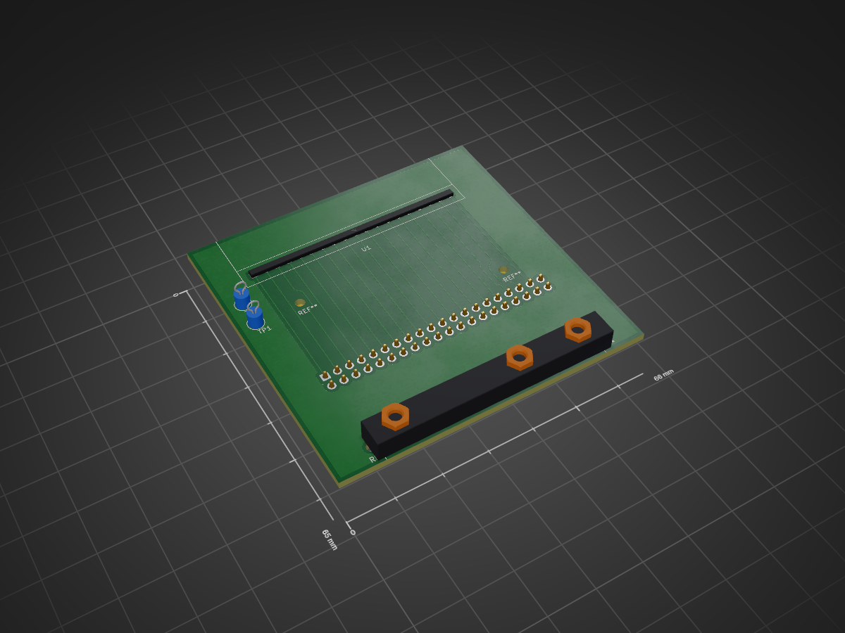
Akashi-10 is an open-source printed circuit board by suikan4github, from the suikan4github/Akashi-10 repository on GitHub, published under the CC0-1.0 licence. It is a 2-layer board of 66 × 65 mm with 12 parts on 40 nets, routed with 94 tracks and 0 vias.
Its parts include 2 connectors and 1 IC.
Test board of the EL-210 calculator
This board is developed to test the functionality of the EL-210 Calculator controller. The EL-210 was released from SHARP Corporation at 1980.
This board tests its internal 9 digits VFD and 9x3 matrix keyboard. All signals and power from internal AA*2 batteries are taken out by 40pin headers.
The ping assignment of the 40pin headers are as followings :
| Pin | Symbol | Pin | Symbol |
|---|---|---|---|
| 1 | H1 | 2 | H2 |
| 3 | a | 4 | |
| 5 | D8 | 6 | R1 |
| 7 | g | 8 | R2 |
| 9 | D7 | 10 | R3 |
| 11 | f | 12 | C8 |
| 13 | D6 | 14 | C7 |
| 15 | e | 16 | C6 |
| 17 | D5 | 18 | C5 |
| 19 | D4 | 20 | C4 |
| 21 | d | 22 | C3 |
| 23 | D3 | 24 | C2 |
| 25 | dp | 26 | C1 |
| 27 | D2 | 28 | C0 |
| 29 | c | 20 | |
| 31 | D1 | 32 | |
| 33 | b | 34 | |
| 35 | D0 | 36 | |
| 37 | H2 | 38 | |
| 39 | H1 | 20 |
Where odd and even pins are signals of the VFD and the key matrix.
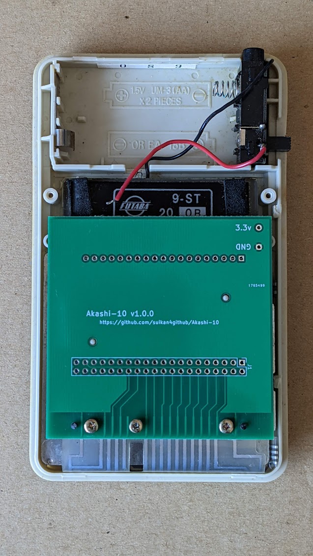
This is photo of the version 1.0.0.
| Qty | Value | Footprint | References |
|---|---|---|---|
| 2 | TestPoint | TestPoint:TestPoint_Loop_D2.60mm_Drill0.9mm_Beaded | TP1, TP2 |
| 1 | 9-ST-20 | 9-ST-20:9-ST-20 | U1 |
| 1 | Conn_02x20_Odd_Even | Connector_PinHeader_2.54mm:PinHeader_2x20_P2.54mm_Vertical | J1 |
| 1 | EL-210-KEY | EL-210-KEY:EL-210-KEY | P1 |
The 5 most common of 12 parts.
It measures 66 × 65 mm and has 2 copper layers, 1.6 mm thick.
12 parts. The full list of its parts is on this page, with links to each part's symbol and footprint where PCBKit's library has them.
From the suikan4github/Akashi-10 repository on GitHub, at the commit this page was made from: the board is Akashi-10.kicad_pcb. PCBKit opens the board in the browser, with nothing to install.
Its repository publishes it under the CC0-1.0 licence: you may reuse it on that licence's terms (keep the author's notice, and for a copyleft licence share your changes alike).
github-linguist/linguist
Language Savant. If your repository's language is being reported incorrectly, send us a pull request!


google/mozc-devices
Circuit diagrams and firmware source code for Gboard DIY keyboards


hackclub/OnBoard
💡 Join 1,000 teenagers and make your first PCB with a $100 grant!

VoronDesign/Voron-Tap
Tap is a nozzle-based z-probe for the V2 and Trident printer designs. The entire toolhead moves to trigger an optical switch. Tap offers many advantages:

stacksmashing/pico-tpmsniffer
A simple, very experimental TPM sniffer for LPC bus