

4 layers42 × 42 mm
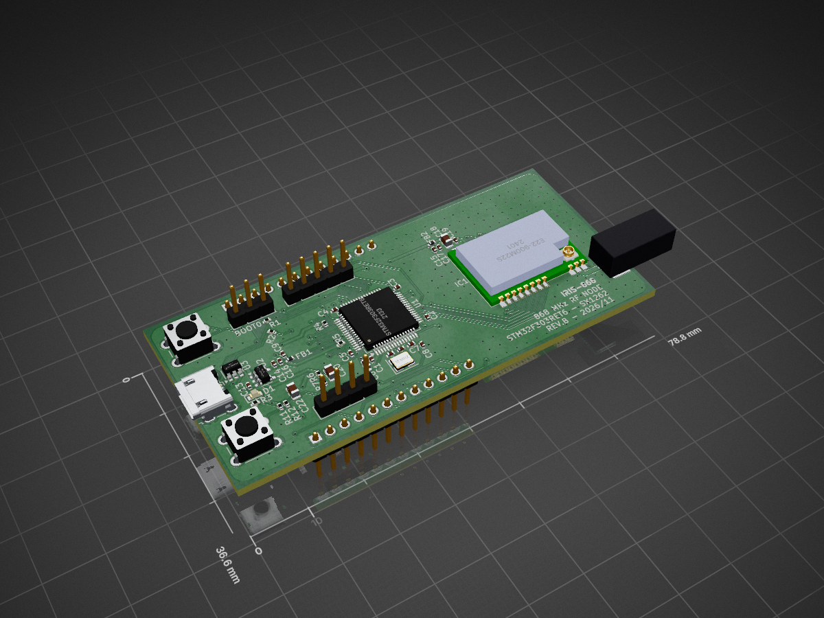
 StringLess80/IRIS-8681
IRIS-868 is a custom embedded RF platform based on the STM32F303RET6 microcontroller and Semtech LLCC68 sub-GHz transceiver, designed for 868 MHz ISM-band wireless communication.
IRIS-868 is an open-source printed circuit board by StringLess80, from the StringLess80/IRIS-868 repository on GitHub. It is a 2-layer board of 78.8 × 36.6 mm with 53 parts on 71 nets, routed with 565 tracks and 327 vias.
It is built around the STM32F303RET6, E22-900M22S and W25Q128JVSIQ, with the AP2112K-3.3 and USBLC6-2SC6 among its other parts. Its parts include 22 capacitors, 13 resistors, 7 connectors, 5 ICs and 2 switches. It belongs with the radio and wireless boards and the STM32 boards of this library.


Custom embedded RF platform for the 868 MHz ISM band
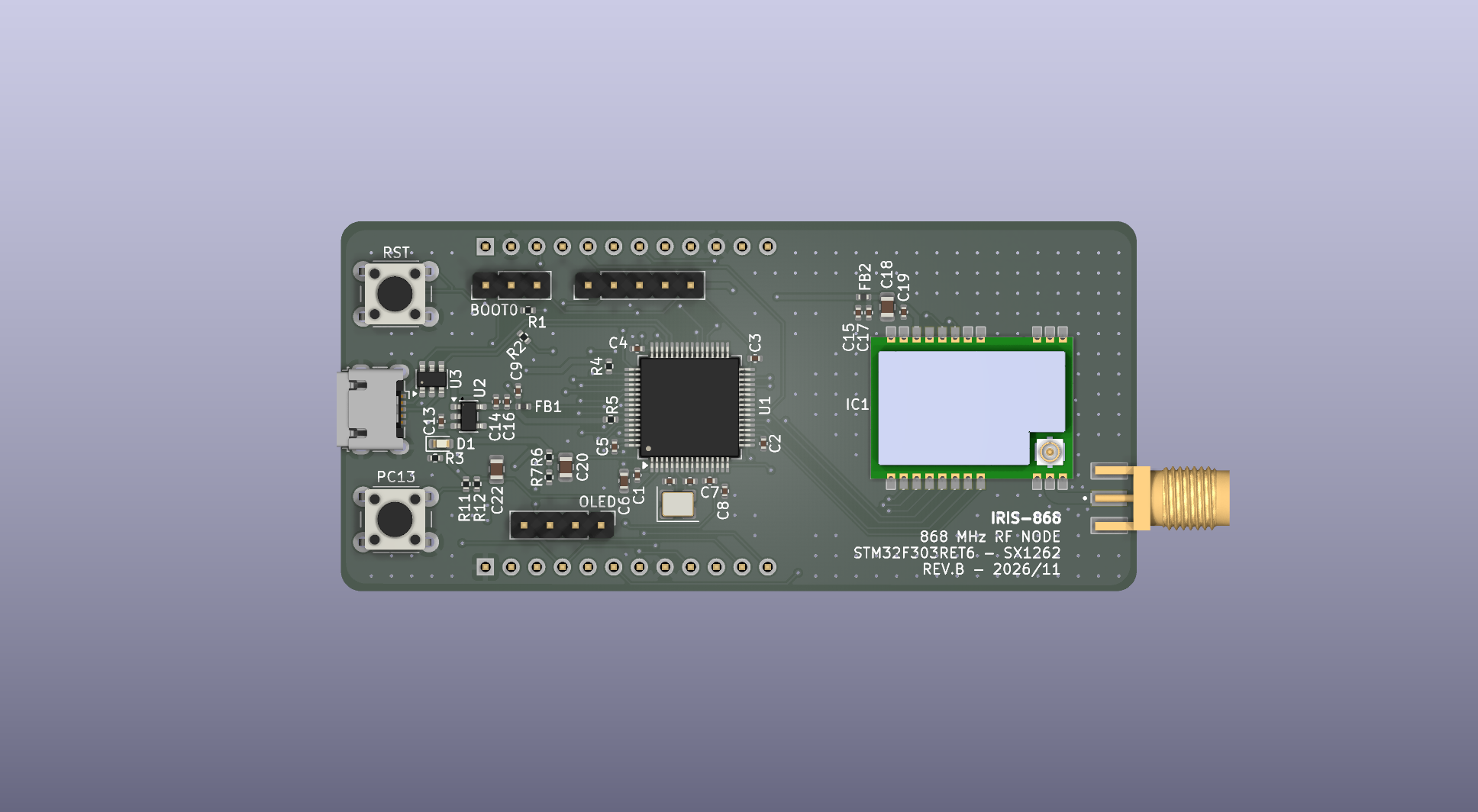
IRIS-868 is a custom embedded RF platform based on the STM32F303RET6 microcontroller and an Ebyte E22-900M22S (Semtech SX1262) sub-GHz LoRa module, designed for 868 MHz ISM-band wireless communication and data logging.










| 🧠 MCU | STM32F303RET6 · Cortex-M4F @ 72 MHz · 512 KB flash · 64 + 16 KB RAM |
| 📻 Radio | Ebyte E22-900M22S · SX1262 · +22 dBm · LoRa / (G)FSK |
| 💾 Storage | Winbond W25Q128JV · 128 Mbit (16 MiB) SPI NOR flash for data logging |
| 🔌 Power | USB micro-B → AP2112K-3.3 LDO, filtered analog and RF rails, VBUS voltage monitoring on the ADC |
| 🧩 Expansion | 2 × 12-pin edge headers · I²C header for 128×64 OLED · 5-pin SWD with NRST · BOOT0 jumper · user button |
| 📐 Board | 2-layer FR4 · 78.8 × 36.6 mm · green mask, white silk · components on both sides |
| 🛠️ Tooling | KiCad 10, footprints and symbols embedded in the project files |
[!WARNING] Revision B is design-complete but has not been bring-up tested. Fabrication files are released as-is. No firmware is included in this repository yet.
| Area | Revision A | Revision B |
|---|---|---|
| Expansion | Most GPIOs unrouted | Two 1×12 edge headers (J5, J7) bring out power, reset, BOOT0, USART1 and 13 GPIOs |
| Debug | 4-pin SWD, no NRST | 5-pin SWD with NRST — "connect under reset" now works |
| Storage | — | 16 MiB W25Q128JV SPI flash on SPI3 (bottom side) |
| User input | Reset button only | Additional user button on PC13 with RC debounce |
| Monitoring | — | VBUS divider (47 kΩ / 15 kΩ) on PC0 for USB voltage measurement |
| USB | D+ pull-up fixed to +3.3 V | D+ pull-up driven by PB8 — firmware-controlled attach/detach |
| Radio | E220-900M22S (LLCC68) | E22-900M22S (SX1262), same MCU connections |
| Boot | BOOT0 floats with no jumper | 100 kΩ pull-down (R13), boots from flash with no jumper |
| Board | 74.2 × 32.0 mm, single-sided assembly | 78.8 × 36.6 mm, bottom-side SMD parts and headers |
A design review before release added these changes:
| Front | Back |
|---|---|
| 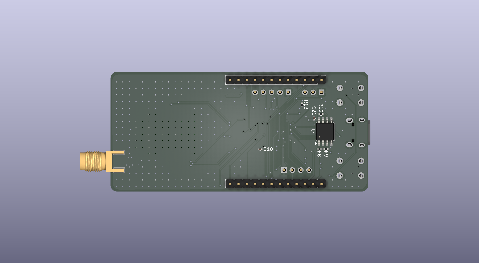 |
📄 Full schematic: docs/schematics/IRIS-868.pdf
flowchart LR
    USB["USB micro-B<br/>J2"] -->|VBUS 5 V| LDO["AP2112K-3.3<br/>600 mA LDO"]
    USB -.->|"D+ / D-"| ESD["USBLC6-2SC6<br/>ESD"]
    ESD -.-> MCU
    USB -->|"VBUS ÷ 4.13"| VMON["V_MON<br/>PC0 / ADC"]
    VMON --> MCU

    LDO --> RAIL(("3.3 V"))
    RAIL -->|"FB1 120 Ω"| VDDA["+3.3VA"]
    RAIL -->|"FB2 120 Ω"| VRF["VRF"]
    RAIL --> MCU
    VDDA --> MCU
    VRF --> MOD

    MCU["STM32F303RET6<br/>Cortex-M4F @ 72 MHz"]
    MCU <-->|"SPI1 · NSS · BUSY · DIO1 · NRST"| MOD["E22-900M22S<br/>SX1262 · +22 dBm"]
    MCU -->|"RXEN / TXEN"| MOD
    MOD -->|ANT| SMA["SMA edge<br/>J6"]

    MCU <-->|"SPI3 · CS"| FLASH["W25Q128JV<br/>16 MiB flash"]
    MCU <-->|"I²C1"| OLED["128×64 OLED<br/>header"]
    MCU <-->|"SWD + NRST"| DBG["ST-Link<br/>J3"]
    MCU <-->|"GPIO · USART1"| HDR["Edge headers<br/>J5 / J7"]
BTN["User button<br/>PC13"] --> MCUIRIS-868/
├── CHANGELOG.md Release history
├── hardware/
│ ├── kicad/ KiCad 10 project (schematic, PCB, design rules)
│ │ └── libs/ Source symbols, footprints, 3D models
│ └── gerbers/
│ ├── rev.A/ Gerber and Excellon files, revision A
│ └── rev.B/ Gerber and Excellon files, revision B
├── production/BOM/ Interactive BOM for assembly
└── docs/
├── schematics/ Schematic PDF
├── images/ Board renders by revision
└── datasheets/ Component reference documentsThe schematic uses four top-level sheets, a KiCad 10 feature: MCU, crystal, reset, VBUS monitor and edge headers (IRIS-868.kicad_sch), power and USB (pwr.kicad_sch), the radio (rf.kicad_sch), and connectors, flash and the user button (interfaces.kicad_sch).
USB VBUS feeds an AP2112K-3.3 LDO (SOT-23-5, 600 mA) that generates the single 3.3 V system rail. Three domains branch from it:
| Rail | Source | Decoupling | Purpose |
|---|---|---|---|
+3.3V | LDO output | 10 µF + 7 × 100 nF + 2 × 1 µF | MCU digital, I/O, flash, headers |
+3.3VA | via FB1 (120 Ω ferrite) | 1 µF + 10 nF | STM32 VDDA / analog reference |
VRF | via FB2 (120 Ω ferrite) | 22 µF + 1 µF + 2 × 100 nF | RF module supply |
The ferrite beads isolate the analog and RF domains from digital switching noise on the main rail, and C7 and C8 sit next to the VDDA pin. The 22 µF bulk capacitor on VRF supplies the current burst drawn by the module during transmission.
VBUS and +3.3 V are both available on header J5, so the board can supply a small carrier or add-on board.
A 47 kΩ / 15 kΩ divider (R6 / R7) scales VBUS onto V_MON (PC0, ADC12_IN6), filtered by C20 (100 nF). The divider ratio is 15 / 62, so 5.0 V on VBUS reads as about 1.21 V, and firmware recovers VBUS as V_MON × 4.133. The divider draws roughly 80 µA from VBUS, and its ~11 kΩ source impedance combined with C20 gives a stable input for the ADC sample-and-hold.
The E22-900M22S connects to the MCU over SPI1 plus four control lines. RXEN and TXEN drive the module's internal RF switch and must be managed by firmware around every transmit/receive transition. The antenna net (ANT) leaves the module's stamp-hole RF pad away from the module body and reaches the SMA edge connector as a 7.4 mm, 1.0 mm-wide coplanar trace on F.Cu, over an unbroken ground plane on B.Cu. A project design rule sets a 0.15 mm gap to the surrounding copper, which gives a calculated impedance of about 50 Ω with a 1.51 mm dielectric and εr 4.5. GND vias flank the feed.
A Winbond W25Q128JVSIQ (SOIC-8, 208 mil) on the bottom side provides 16 MiB of non-volatile storage on SPI3 (PC10 / PC11 / PC12) with chip select on PD2. The CS line has a 10 kΩ pull-up (R8) so the flash stays deselected while the MCU is in reset. /WP and /HOLD are tied high through R9 and R10, so the device operates in standard single-bit SPI mode; dual/quad I/O is not available on this revision. C21 decouples the flash locally.
| Button | Net | Circuit |
|---|---|---|
| SW1 (RST) | NRST (pin 7) | Pulls NRST low. 100 nF (C10) sits next to the pin on the bottom side. NRST is also on the SWD header and J5 |
| SW2 (PC13) | PC13 (pin 2) | Active-low. 10 kΩ pull-up (R11), 10 kΩ series (R12), 100 nF (C22) to GND — about 1 ms fall / 2 ms rise debounce |
The USB D+ 1.5 kΩ pull-up (R2) is connected to PB8 rather than to +3.3 V. Firmware must drive PB8 high to signal device attach to the host, and can drive it low to force a clean disconnect/re-enumeration without unplugging the cable.
| Connector | Type | Pinout |
|---|---|---|
| J2 USB | micro-B | USB FS device on PA11/PA12, D+ pull-up switched by PB8, ESD-protected |
| J3 SWD | 1×5 @ 2.54 mm | GND · NRST · SWCLK · SWDIO · +3.3V |
| J1 (BOOT0) | 1×3 @ 2.54 mm | GND · BOOT0 · +3.3V — no jumper or 1–2 = flash, 2–3 = bootloader |
| J4 (OLED) | 1×4 @ 2.54 mm | GND · +3.3V · SCL · SDA (1.5 kΩ pull-ups on board) |
| J5 | 1×12 @ 2.54 mm, bottom-mounted | Power, reset, BOOT0, USART1, GPIO — see below |
| J7 | 1×12 @ 2.54 mm, bottom-mounted | GPIO — see below |
| J6 SMA | edge-mount | Antenna |
J5 and J7 run along the long edges of the board with a row-to-row spacing of 31.75 mm (1.25 in). The header bodies are mounted on the bottom side, so the board can be plugged into a carrier with the components facing up. Pin 1 of each header is at the USB end.
| Pin | J5 | J7 |
|---|---|---|
| 1 | GND | PB9 |
| 2 | +3.3V | GND |
| 3 | VBUS (5 V) | PB0 |
| 4 | NRST | PB1 |
| 5 | BOOT0 | PC4 |
| 6 | PA9 (USART1_TX) | PC5 |
| 7 | PA10 (USART1_RX) | PC6 |
| 8 | GND | PC7 |
| 9 | PB4 | PC8 |
| 10 | PB5 | GND |
| 11 | PB6 | not connected |
| 12 | PB8 ⚠️ USB D+ pull-up | not connected |
| STM32 pin | Signal | Module pin | Direction | Function |
|---|---|---|---|---|
PA5 | SPI1_SCK | 18 (SCK) | → | SPI clock |
PA6 | SPI1_MISO | 16 (MISO) | ← | SPI data out |
PA7 | SPI1_MOSI | 17 (MOSI) | → | SPI data in |
PA4 | NSS | 19 (NSS) | → | Chip select, active low |
PA3 | NRST | 15 (NRST) | → | Module reset, active low |
PA2 | BUSY | 14 (BUSY) | ← | Transceiver busy status |
PA8 | DIO1 | 13 (DIO1) | ← | Primary interrupt line |
PB10 | RXEN | 6 (RXEN) | → | RF switch, receive enable |
PB11 | TXEN | 7 (TXEN) | → | RF switch, transmit enable |
Module pin 8 (DIO2) is left unconnected in revision B.
| STM32 pin | Signal | Flash pin | Direction |
|---|---|---|---|
PC10 | SPI3_SCK | 6 (CLK) | → |
PC11 | SPI3_MISO | 2 (DO) | ← |
PC12 | SPI3_MOSI | 5 (DI) | → |
PD2 | FLASH_CS | 1 (/CS) | → |
| STM32 pin | Function |
|---|---|
PA11 / PA12 | USB D− / D+ |
PB8 | USB D+ pull-up control (also on J5 pin 12) |
PA13 / PA14 | SWDIO / SWCLK |
PA15 | I²C1 SCL (AF4) |
PB7 | I²C1 SDA (AF4) |
PC0 | V_MON — VBUS voltage divider (ADC) |
PC13 | User button, active low |
PF0 / PF1 | 16 MHz crystal (OSC_IN / OSC_OUT) |
NRST (pin 7) | Reset button + 100 nF, SWD header, J5 |
BOOT0 (pin 60) | J1 via 10 kΩ (R1), 100 kΩ pull-down (R13), J5 (direct) |
PA9, PA10, PB4–PB6 | J5 |
PB0, PB1, PB9, PC4–PC8 | J7 |
The remaining GPIOs — PA0, PA1, PB2, PB3, PB12–PB15, PC1–PC3, PC9, PC14, PC15 — are not routed in revision B.
| Parameter | Value |
|---|---|
| Dimensions | 78.8 × 36.6 mm, 2 mm corner radius |
| Layers | 2 (F.Cu / B.Cu), GND pour on both |
| Stackup | 1.6 mm FR4, 35 µm copper, εr 4.5 |
| Finish | HASL, green solder mask, white silkscreen |
| Vias | 327, 0.6 mm with 0.3 mm drill, tented |
| Minimum rules | Track 0.15 mm, clearance 0.2 mm, annular ring 0.13 mm, hole-to-hole 0.5 mm, copper-to-edge 0.2 mm |
| Assembly | Double-sided (U4, R8–R10, R13, C10, C21 and header bodies on the bottom) |
| Special rules | 0.15 mm clearance on the ANT coplanar feedline |
| Ref | Qty | Value | Package | Notes |
|---|---|---|---|---|
| U1 | 1 | STM32F303RET6 | LQFP-64 | 0.5 mm pitch |
| U2 | 1 | AP2112K-3.3 | SOT-23-5 | 600 mA LDO |
| U3 | 1 | USBLC6-2SC6 | SOT-23-6 | USB ESD protection |
| U4 | 1 | W25Q128JVSIQ | SOIC-8 5.3 × 5.3 mm | 128 Mbit SPI flash, bottom side |
| IC1 | 1 | E22-900M22S | Ebyte SMD module | SX1262, +22 dBm |
| Y1 | 1 | 16 MHz | 3225-4pin | CL ≈ 10 pF, ≤20 ppm recommended |
| C1–C5, C10, C16, C17, C19, C21 | 10 | 100 nF | 0402 | 16 V X7R — C10 and C21 on bottom side |
| C20, C22 | 2 | 100 nF | 0805 | 16 V X7R — V_MON filter, PC13 debounce |
| C8, C9, C14, C15 | 4 | 1 µF | 0402 | 16 V X5R/X7R |
| C13 | 1 | 1 µF | 0402 | 25 V — sits on the 5 V VBUS rail |
| C6 | 1 | 10 µF | 0603 | 16 V X5R |
| C18 | 1 | 22 µF | 0805 | 16 V X5R, RF bulk |
| C7 | 1 | 10 nF | 0402 | 16 V X7R, VDDA filter |
| C11, C12 | 2 | 12 pF | 0402 | 50 V C0G/NP0 ±5%, crystal load |
| R1 | 1 | 10 kΩ | 0402 | BOOT0 series |
| R2 | 1 | 1.5 kΩ | 0402 | USB D+ pull-up (to PB8) |
| R3 | 1 | 1.5 kΩ | 0402 | Power LED series |
| R4, R5 | 2 | 1.5 kΩ | 0402 | I²C pull-ups |
| R6 | 1 | 47 kΩ | 0402 | VBUS divider, top — 1% recommended |
| R7 | 1 | 15 kΩ | 0402 | VBUS divider, bottom — 1% recommended |
| R8, R9, R10 | 3 | 10 kΩ | 0402 | Flash /CS, /WP, /HOLD pull-ups, bottom side |
| R11, R12 | 2 | 10 kΩ | 0402 | PC13 button pull-up / series |
| R13 | 1 | 100 kΩ | 0402 | BOOT0 pull-down, bottom side |
| FB1, FB2 | 2 | 120 Ω @ 100 MHz | 0402 | Analog / RF rail filtering, rated ≥ 500 mA |
| D1 | 1 | Red LED | 0603 | Power indicator |
| SW1, SW2 | 2 | Tactile switch | 6 mm THT | 4-pin, 4.5 × 6.5 mm, marked RST and PC13 |
| J1 | 1 | Pin header 1×3 | 2.54 mm | BOOT0 select, marked BOOT0 |
| J2 | 1 | USB micro-B | Würth 629105150521 | |
| J3 | 1 | Pin header 1×5 | 2.54 mm | SWD + NRST |
| J4 | 1 | Pin header 1×4 | 2.54 mm | I²C / OLED, marked OLED |
| J5, J7 | 2 | Pin header 1×12 | 2.54 mm | Edge headers, bottom side |
| J6 | 1 | SMA edge-mount | RF Solutions CON-SMA-EDGE-S |
For assembly, open the interactive BOM after downloading it.
[!TIP] Capacitor voltage ratings account for MLCC DC bias derating — class II ceramics lose a large fraction of their nominal capacitance near their rated voltage, so ratings are specified at roughly 4–5× the working voltage. A 2.54 mm jumper shunt on J1 is needed only to enter the bootloader, and it isn't part of the PCB BOM.
Fabrication files for revision B are in hardware/gerbers/rev.B/, as Gerber and Excellon drill files. A ready-to-upload zip is attached to the v2.0.0 release.
The project requires KiCad 10 or later, because it uses multiple top-level sheets. Symbols and footprints are embedded in the project files, so it opens without any library setup. Sources for the non-standard parts (E22 module, SMA edge connector) and the 3D models are under hardware/kicad/libs/. DRC reports one library warning on J6, because its source library is not registered in the project.
git clone https://github.com/StringLess80/IRIS-868.git
cd IRIS-868
kicad hardware/kicad/IRIS-868.kicad_proVia SWD (recommended) — connect an ST-Link or any CMSIS-DAP probe to J3, including the NRST line. Because NRST is on the header, "connect under reset" works, so a board with firmware that disables SWD or enters low-power mode early can still be recovered from the debugger.
st-flash --reset write firmware.bin 0x08000000Via UART bootloader — connect a 3.3 V USB-serial adapter to J5 (PA9 = MCU TX, PA10 = MCU RX, GND), fit the J1 jumper on pins 2–3 and reset:
stm32flash -w firmware.bin -v -g 0x0 /dev/ttyUSB0Via USB DFU — the ROM bootloader does not drive PB8, so the D+ pull-up is inactive and the host will not see the device. Tie J5 pin 12 (PB8) to J5 pin 2 (+3.3V) for the duration of the DFU session, fit the J1 jumper on pins 2–3, reset, then:
dfu-util -a 0 -s 0x08000000:leave -D firmware.bin[!CAUTION] Remove the PB8 link before running application firmware — if firmware drives PB8 low while it is tied to +3.3 V, the pin is shorted.
Remove the jumper, or move it to pins 1–2, and reset to run from flash.
| Version | Hardware | Status |
|---|---|---|
v2.0.0 | Revision B | Released for fabrication, not bring-up tested |
v1.0.0 | Revision A | Superseded |
The major version changes with each PCB revision. Minor and patch versions cover compatible changes to the BOM, documentation or fabrication outputs. See the changelog for details.
Made with KiCad 🛠️
| Qty | Value | Footprint | References |
|---|---|---|---|
| 10 | 100 nF | Capacitor_SMD:C_0402_1005Metric | C1, C2, C3, C4, C5, C10, C16, C17, C19, C21 |
| 5 | 1 uF | Capacitor_SMD:C_0402_1005Metric | C8, C9, C13, C14, C15 |
| 5 | 10k | Resistor_SMD:R_0402_1005Metric | R8, R9, R10, R11, R12 |
| 4 | 1k5 | Resistor_SMD:R_0402_1005Metric | R2, R3, R4, R5 |
| 2 | 100 nF | Capacitor_SMD:C_0805_2012Metric | C20, C22 |
| 2 | 12 pF | Capacitor_SMD:C_0402_1005Metric | C11, C12 |
| 2 | 120 R | Inductor_SMD:L_0402_1005Metric | FB1, FB2 |
| 2 | Conn_01x12_Pin | Connector_PinHeader_2.54mm:PinHeader_1x12_P2.54mm_Vertical | J5, J7 |
| 1 | 10 k | Resistor_SMD:R_0402_1005Metric | R1 |
| 1 | 10 nF | Capacitor_SMD:C_0402_1005Metric | C7 |
| 1 | 10 uF | Capacitor_SMD:C_0603_1608Metric | C6 |
| 1 | 100k | Resistor_SMD:R_0402_1005Metric | R13 |
| 1 | 128x64 OLED | Connector_PinHeader_2.54mm:PinHeader_1x04_P2.54mm_Vertical | J4 |
| 1 | 15k | Resistor_SMD:R_0402_1005Metric | R7 |
| 1 | 16 MHz | Crystal:Crystal_SMD_3225-4Pin_3.2x2.5mm | Y1 |
| 1 | 22 uF | Capacitor_SMD:C_0805_2012Metric | C18 |
| 1 | 47k | Resistor_SMD:R_0402_1005Metric | R6 |
| 1 | AP2112K-3.3 | Package_TO_SOT_SMD:SOT-23-5 | U2 |
| 1 | BTN | Button_Switch_THT:SW_PUSH_6mm | SW2 |
| 1 | E22-900M22S | E22-900M22S:E22-900M22S | IC1 |
| 1 | PRG | Connector_PinHeader_2.54mm:PinHeader_1x03_P2.54mm_Vertical | J1 |
| 1 | RED | LED_SMD:LED_0603_1608Metric | D1 |
| 1 | RST | Button_Switch_THT:SW_PUSH_6mm | SW1 |
| 1 | SMA | CON-SMA-EDGE-S:RFSOLUTIONS_CON-SMA-EDGE-S | J6 |
| 1 | STM32F303RET6 | Package_QFP:LQFP-64_10x10mm_P0.5mm | U1 |
| 1 | SWD | Connector_PinHeader_2.54mm:PinHeader_1x05_P2.54mm_Vertical | J3 |
| 1 | USBLC6-2SC6 | Package_TO_SOT_SMD:SOT-23-6 | U3 |
| 1 | USB_B_Micro | Connector_USB:USB_Micro-B_Wuerth_629105150521 | J2 |
| 1 | W25Q128JVSIQ | Package_SO:SOIC-8_5.3x5.3mm_P1.27mm | U4 |
It measures 78.8 × 36.6 mm and has 2 copper layers, 1.6 mm thick.
53 parts, built around the STM32F303RET6, E22-900M22S, W25Q128JVSIQ and AP2112K-3.3. The full list of its parts is on this page, with links to each part's symbol and footprint where PCBKit's library has them.
From the StringLess80/IRIS-868 repository on GitHub, at the commit this page was made from: the board is hardware/kicad/IRIS-868.kicad_pcb and its schematic hardware/kicad/IRIS-868.kicad_sch. PCBKit opens the board in the browser, with nothing to install.
Its repository states no licence, so its author keeps all rights: ask StringLess80 before reusing the design.


gmlewis/asic-reticulum
SpinalHDL implementation of ASIC hardware for go-reticulum


trabem/home_sense_meteostation
Репозиторій автономної battery-powered метеостанції на ESP32-C3-WROOM-02. Містить firmware (ESP-IDF / FreeRTOS), KiCad-проєкти двох плат і матеріали фінальної презентації.


DashiellRussell/UNSW_Rocketry_Senior_Flight_Computer
KiCad project for the senior flight computer used by UNSW Rocketry.