2 layers40 × 30 mm

 steieio/swd-blaster5
This design adapts the 10 pin 50 mil picth JTAG header pinout used by Arm to the 10 pin 100 mil pitch header pinout used by Altera for their Blasters. It works great with the Tigard board and openFPGALoader.
Swd blaster is an open-source printed circuit board by steieio, from the steieio/swd-blaster repository on GitHub, published under the CC0-1.0 licence. It is a 2-layer board of 12.7 × 22.2 mm with 3 parts on 11 nets, routed with 44 tracks and 4 vias.
It belongs with the interfaces and adapters boards of this library.
This design adapts the 10 pin 50 mil picth JTAG header pinout used by Arm to the 10 pin 100 mil pitch header pinout used by Altera for their Blasters. It works great with the Tigard board and openFPGALoader.
You can order the PCB inexpensively from OSH Park. I've included a PDF version of the schematic for convenience.
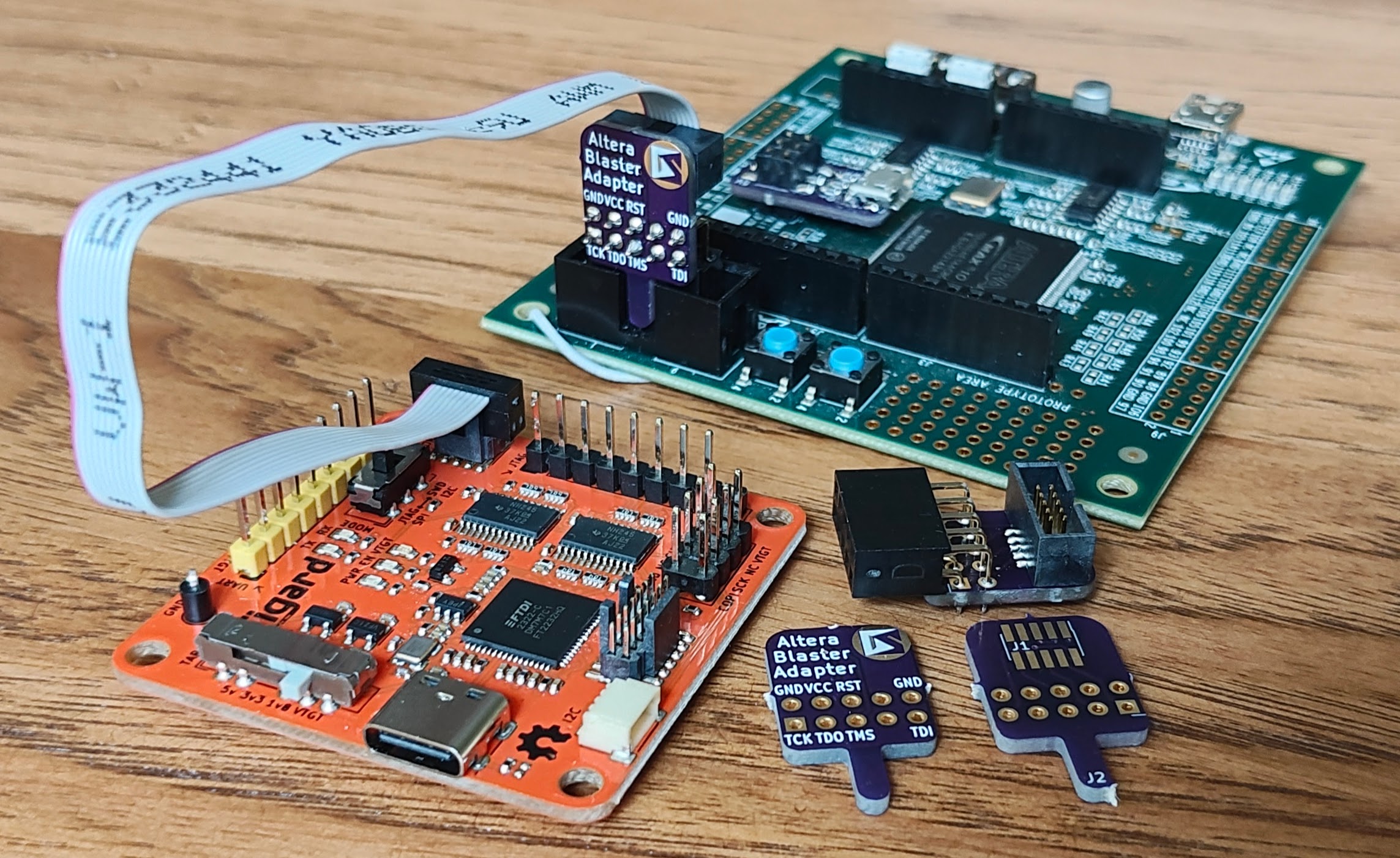
Here is the board being used to connect Tigard to the MAX10 10M08 Evaluation Kit:
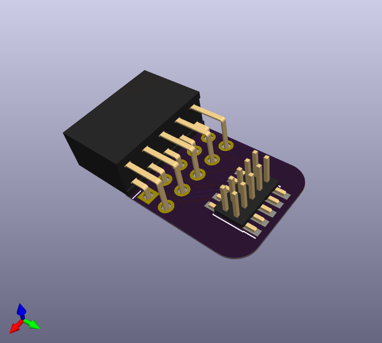
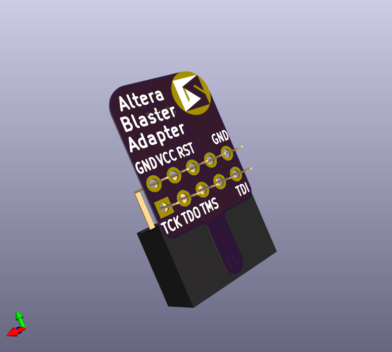
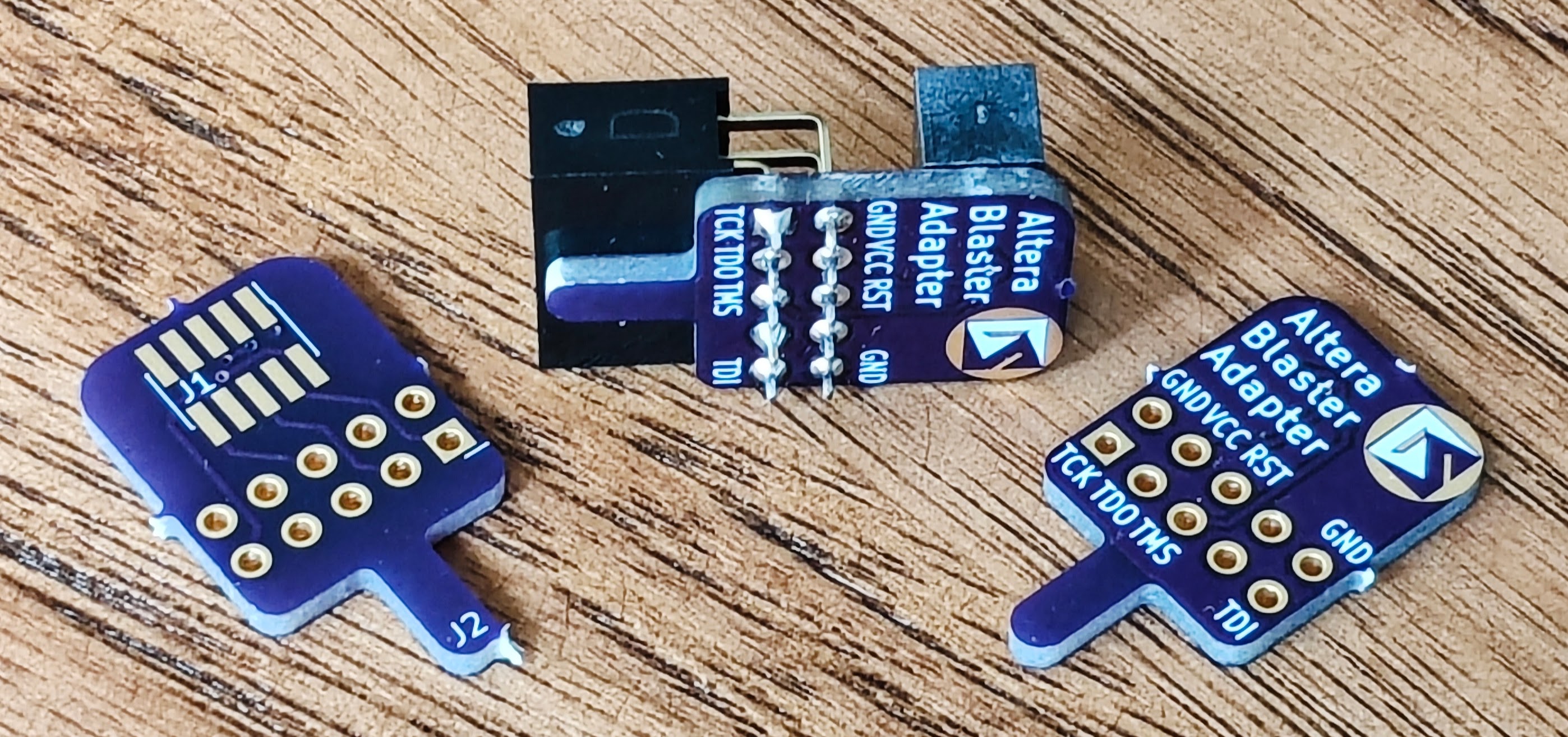
Here are some additional images of the board:
| Qty | Value | Footprint | References |
|---|---|---|---|
| 1 | Conn_02x05_Counter_Clockwise | custom:PinSocket_2x05_P100mil_Board_Tab | J2 |
| 1 | Conn_02x05_Counter_Clockwise | Connector_PinHeader_1.27mm:PinHeader_2x05_P1.27mm_Vertical_SMD | J1 |
| 1 | GS_logo | custom:gs_logo_200mil | GS1 |

hzeller/rpi-rgb-led-matrix
Controlling up to three chains of 64x64, 32x32, 16x32 or similar RGB LED displays using Raspberry Pi GPIO


atopile/atopile
Design circuit boards with code! ✨ Get software-like design reuse 🚀, validation, version control and collaboration in hardware; starting with electronics ⚡️


hackclub/sprig
🍃 Learn to code by making games in a JavaScript web-based game editor.
It measures 12.7 × 22.2 mm and has 2 copper layers, 0.19 mm thick.
3 parts. The full list of its parts is on this page, with links to each part's symbol and footprint where PCBKit's library has them.
From the steieio/swd-blaster repository on GitHub, at the commit this page was made from: the board is swd-blaster.kicad_pcb and its schematic swd-blaster.kicad_sch. PCBKit opens the board in the browser, with nothing to install.
Its repository publishes it under the CC0-1.0 licence: you may reuse it on that licence's terms (keep the author's notice, and for a copyleft licence share your changes alike).