2 layers270 × 100 mm
FCU Mainboard v3
stefanofinetti/MF_A320_Glareshield
Complete project for the MobiFlight FCU/EFIS Mainboard
143 partsGPL-3.0
 stefanofinetti/MF_A320_Glareshield
Complete project for the MobiFlight FCU/EFIS Mainboard
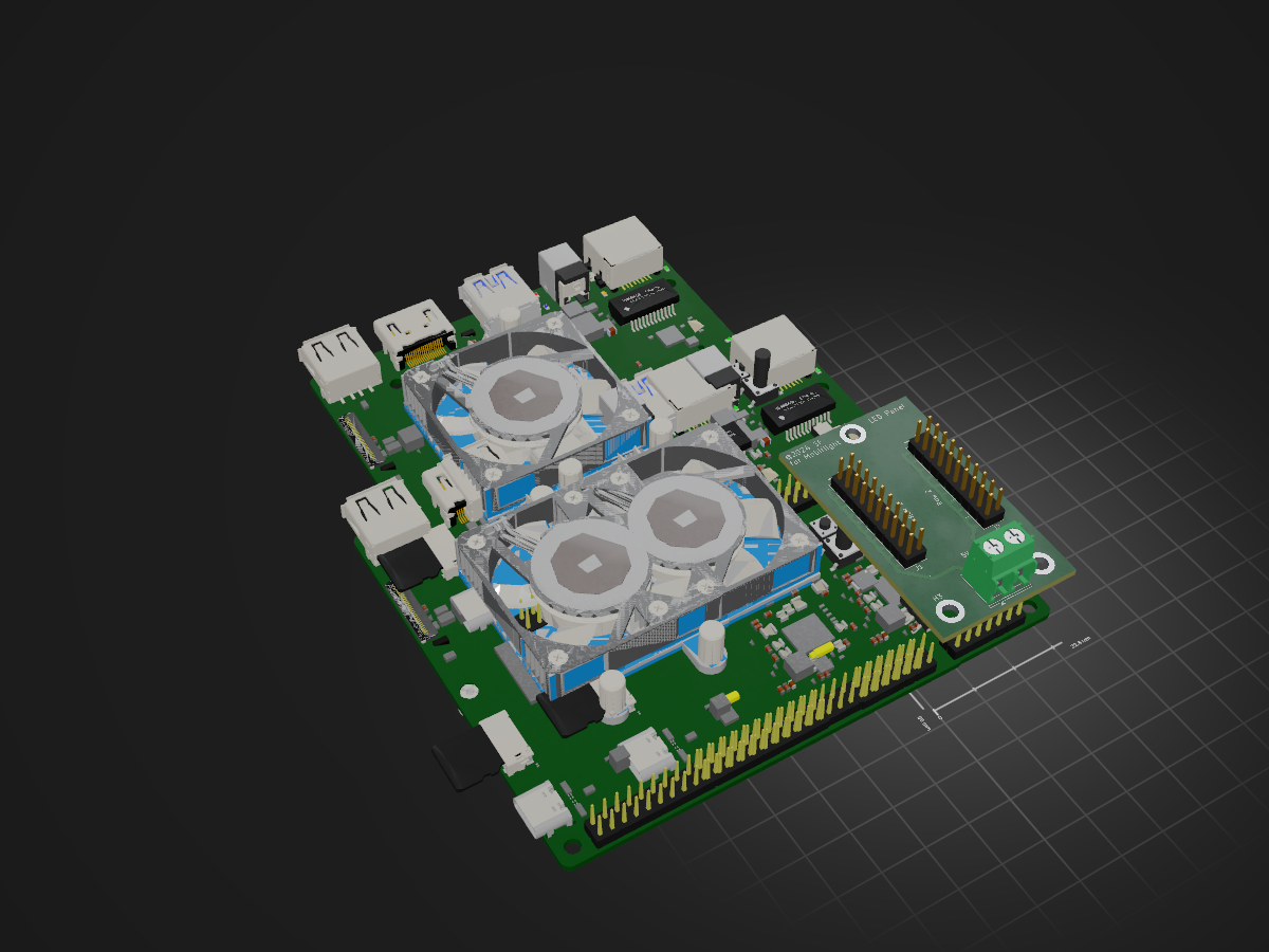
Backlighting LEDModule PCB is an open-source printed circuit board by stefanofinetti, from the stefanofinetti/MF_A320_Glareshield repository on GitHub, published under the GPL-3.0 licence. It is a 2-layer board of 32.3 × 55 mm with 6 parts on 2 nets, routed with 128 tracks and 0 vias.
This repository contains the complete glareshield unit: the FCU in the centre and the two EFIS control panels either side, driven by MobiFlight. The two outer side panels are not built — three rarely used buttons did not justify the plastic.
The unit sits on a desk, is powered by its own mains adapter and connects to the PC over USB, so it can be unplugged and moved.
| Folder | Project | Qty | Role |
|---|---|---|---|
Mainboard/ | FCU_Mainboard_v3 | 1 | ATmega2560 + CH340G, 7 OLEDs behind a PCA9548A I²C mux, 4× CD74HC4067 analogue mux for the buttons, 20 annunciator outputs, TPS2115A supply selector. 270 × 100 mm, 2 layers |
PSU/ | 9V_Distribution | 1 | 70 × 80 mm. Two independent regulators off one 9 V input: an LM2596S-5 buck for the backlighting and a P78A05-1000 for the mainboard. See PSU revision below |
Backlighting_Dimmer/ | Backlighting_PCB | 1 | NE555 PWM dimmer, potentiometer controlled, IRLIZ44N low-side switch, three outputs |
Backlighting_LEDModule/ | Backlighting_LEDModule_PCB | 3 | Passive fan-out: one input → twenty 2-pin outputs. Three of them only to keep the LED strip wiring short |
Korry_Large/ | KorryLargePCB_SMD | — | Tactile switch + green annunciator LED + white backlight LED |
Korry_Small/ | KorrySmallPCB_SMD | — | Same, smaller outline |
 mains adapter 9 V / 3 A
        │
        └──► PSU  J1 ──► D1 ──┬──► F2 ──► LM2596S-5 ──► L1 ──┬──► 5 V ──┬──► J2 ─┐
                              │   (2 A)     D2 ◄──┘          │          ├──► J3 ─┤
                              │             catch      C2 ‖ C4          └──► J4 ─┤
                              │                                                  │
                              └──► F3 ──► P78A05-1000 ──► J5 ──► Mainboard J13    │
                                 (0.5 A)   C5‖C6  C7‖C8                  │        │
                                                                     IN1 ▼        │
 PC ──USB──► Mainboard P1 ──► VBUS ──────────────► IN2 ──► U8 TPS2115A            │
   (powered USB3 hub)                                         OUT ──► +5V         │
        │                                                                         │
        └──► 20 × Korry  (green annunciator LED + button)                         │
                   │                                                              │
                   │                            Backlighting_Dimmer ◄─────────────┘
                   │                                    │
                   │                                    └──► 3 × LEDModule
                   └──────────── white backlight LED ◄───────────┘
                                 + 6 LED strip segments
Two supply chains that share only ground. The backlighting, which draws the
real current, runs off the mains adapter through the buck. The mainboard takes
whichever of the two is available: U8 picks the adapter through J13
whenever it is plugged in and falls back to USB when it is not — see
Mainboard selector.
Every cable in the unit is straight through: pin 1 to pin 1. It was not always so, and the boards still carry the marks that say which pin is which, so you can check rather than trust this page.
BTN+LED, 3-pin)| pin | Signal | Marked |
|---|---|---|
| 1 | GND | GND on the mainboard, G on the Korry |
| 2 | annunciator LED, driven by an MCU pin through the 220 Ω on the Korry board | LED / L |
| 3 | button to GND, read through a CD74HC4067 | BTN / B |
BK_LED, 2-pin)| pin | Signal | Marked |
|---|---|---|
| 1 | +5 V | + on the odd row of the LEDModule, + on the Korry |
| 2 | switched return, through the 91 Ω on the Korry board | - |
BOARD_CONN, screw terminal)| pin | Signal |
|---|---|
| 1 | +5 V, always present |
| 2 | return, switched to GND by the IRLIZ44N |
The dimmer's three outputs are marked TO LEDMODULE, the LEDModule's input
5V IN, and both have a + and a - next to the screws.
J2, J3 and J4 are three taps on one node, not three independent lines.
There is no per-output fusing. Protection is per branch, not per output:
F2 (2 A) covers everything downstream of the buck, F3 (0.5 A) covers the
mainboard regulator, and a fault on one cannot take the other down.
Calculated where the resistors are known, estimated elsewhere.
| Load | Rail | Current |
|---|---|---|
| 7 OLEDs | +3V3, from +5V through the AMS1117 | 105–140 mA |
| Green annunciators, 11 lit worst case (220 Ω) | driven by MCU pins | ~130 mA |
| ATmega2560 + CH340G + muxes + power LED | VIN / +5V | ~55 mA |
| Mainboard total, from USB | 290–340 mA | |
| 20 white backlight LEDs (91 Ω) | backlight 5 V | 418 mA |
| 6 LED strip segments, 3528 | backlight 5 V | 360–720 mA |
| Backlighting total, from the adapter | 780–1140 mA |
The adapter supplies 27 W and the unit uses under 7 W. Nothing is binding any
more: F2 was the constraint when it was a 1 A part, which derated to under
0.8 A of hold current against the 0.75 A the buck actually draws. At 2 A it
has margin to spare.
The 9 V distribution board was reworked.
| Change | Why |
|---|---|
D2 added — 1N5822, cathode on the switch node, anode to ground | A non-synchronous buck has nowhere for the inductor current to go when the switch opens. Without an external diode it freewheels through the substrate diode of the LM2596 itself: roughly 0.4 W of extra dissipation inside the package on top of its own 0.7 W, and substrate injection the part is not specified for. This is why the board works and why it degrades |
C4 added — 220 µF radial electrolytic in parallel with C2 | The LM2596 control loop needs some ESR on the output, and C2 was a ceramic with almost none. C2 has since become an electrolytic too, so the two now share the job. The RMP V5, same family of design but with electrolytics at its regulator, has never misbehaved |
F2 1 A → 2 A (MF-RHT100 → MF-RHT200) | At 1.14 A out the input draws about 0.75 A. Derated for the temperature inside a printed case, a 1 A polyfuse holds under 0.8 A — too close to nuisance tripping. Pads are identical, so the swap costs nothing in layout |
| Power section re-laid out | U4 pin 2, the cathode of D2 and pin 1 of L1 now sit on one straight line at y = 64.95, and C1 sits 4 mm under the VIN pin. The commutation loop went from nonexistent to about 4 mm of forward track each side |
D1, D2, C1 and C2 were SMD; they are now through-hole. Two of those
four are not a convenience:
C1 sits across the 9 V input and needs 25 V of rating. A 1206 MLCC of
that capacitance does not exist at 25 V, so the part was always going to be
under-rated and to lose most of its capacitance to DC bias. As a radial
electrolytic the problem simply goes away.C2 is the buck's output capacitor, and the LM2596 wants some ESR there.
As a ceramic it had almost none, which is why C4 was added; as an
electrolytic it provides it itself.D1 and D2 are 1N5822, 40 V 3 A, which is generous against the ~1 A each
actually carries. D2 is mounted vertically on a 5.08 mm pitch, shorter than
the 6.8 mm of the SMC it replaces, so the commutation loop got slightly
tighter rather than longer.
Everything in the buck section is now through-hole except U4, whose tab
needs the copper pour to dissipate, and the status LEDs with their resistors.
A useful side effect: every ground pad in that section now passes through the
board and reaches both planes on its own, so four stitching vias and their
stubs are gone.
Component spacing was opened up at the same time. Nothing placed by hand is closer than 2 mm to its neighbour now; the tightest pairs left on the board are the original LED-and-resistor pairs at 0.66 mm.
The mainboard needs a 5 V source that does not depend on the USB hub. It does
not take it from J2/J3/J4: those are one node with the backlighting
on it, PWM-switched by the dimmer's IRLIZ44N in steps of up to 1.1 A. Putting
the MCU and seven OLEDs on that rail would feed them those steps.
Instead a second, independent regulator, tapped from D1's cathode: the reverse
protection is shared, the fuse is not, so a fault on one branch cannot take
down the other. F3 is 0.5 A for the branch's ~215 mA at 9 V. U1 is the same
P78A05-1000 module used on RMP V5, with 100 nF + 100 uF each side as there.
The board grew from 50 × 70 to 70 × 80 mm to make room. The whole regulator chain lives in the new strip at x 150..170, so the buck section keeps its original placement and its original routing, and every track stays on the front: the bottom layer is an uninterrupted ground plane.
All 55 tracks are on the front, so the return current of each loop runs
directly beneath its outward track and the enclosed area stays small.
Stitching vias next to the ground terminals of C1, C2, C4 and the anode
of D2 are tied to their pads by short tracks rather than through the
thermal spokes.
The outline and the four mounting holes did move with the enlargement, so the
printed base has to be reprinted or its brass inserts moved. The positions of
J1 to J4 are unchanged, so the wiring loom stays as it is.
U8 is a TPS2115A power mux: IN1 takes the clean 5 V from the PSU's J5,
IN2 takes USB VBUS, and OUT becomes the board's +5V. D0 is tied to ground and D1 comes from a 100k/100k divider
on the incoming rail, which makes the choice deterministic rather than
"whichever input happens to be higher": the external supply wins whenever it
is above about 4 V, and the board falls back to USB below that.
The part has no body diodes across its switches, so nothing can flow back
into the USB port when the board runs on the adapter. ILIM is set to about
0.8 A by R34. STAT is left unconnected; it is an open-drain output that
goes low on IN1, if an indicator is ever wanted.
P1 pin 1 and R14, the D+ pull-up, moved off +5V onto the new VBUS
net. JP1, VCC and the ISP path are untouched: JP1 still chooses whether
VIN comes from the board rail or from the programmer.
The symbol lives in Mainboard/TPS2115A.kicad_sym with a project-local
sym-lib-table, so the repository is self-contained.
Counting tracks as well as footprints, the old 250 mm board had no free rectangle big enough for the cluster anywhere near the power section, so the board grew to 270 x 100 mm: it gains 20 mm on the right and nothing that already existed moves, apart from the two right-hand mounting holes, which go from x 265 to x 285. The other five stay put. The 100 mm depth is untouched.
The whole selector sits in that new strip, in a column from J13 at the top
down through U8, C27 and the divider.
The cluster is routed and the board reports 0 violations, 0 unconnected items and 0 parity issues.
The three power connections around the selector run at 1 mm, the width their netclass asks for. They cannot run that wide the whole way: they leave pins 6, 7 and 8 of a TSSOP at 0.65 mm pitch, where the pad itself is only 0.4 mm tall, so each stays at 0.4 mm for the three to six millimetres it travels alongside the other two and widens as soon as they diverge. Series resistance of the three paths, in 35 µm copper:
| Path | |
|---|---|
5V_EXT, J13 → U8 pin 8 | 19 mΩ |
+5V, U8 pin 7 → C27 | 13 mΩ |
VBUS, C26 → U8 pin 6 | 13 mΩ |
The 5V_EXT spine below y 55 and the tap to R32 stay at 0.3 mm on purpose:
from there down only the SEL divider draws, which is microamps.
The silkscreen is meant to be enough on its own: every connector says what plugs into it and every pin says what it carries, so you can wire the unit with the boards in front of you and the schematic only for the details.
| Board | What is printed |
|---|---|
Mainboard | the function on each connector (APPR, R_FD, HDG_ENC…) and, next to the pins, GND / LED / BTN, L / R on the encoders, VOR / ADF, hPa / inHg. J13 carries 5V from PSU with GND and 5V on its two screws |
PSU | 9V IN on J1, 5V BACKLIGHT on J2–J4, 5V MAINBOARD on J5, and a + beside the live screw of every terminal |
Backlighting_Dimmer | 5V IN on the input, TO LEDMODULE on the three outputs, Backlighting POT on the potentiometer header |
Backlighting_LEDModule | 5V IN on the input, + and - beside its screws and beside both output rows |
Korry_Large | BTN+LED and BK_LED on the two connectors, G, L and B beside pins 1, 2 and 3, + and - beside the backlight connector and beside each LED on the back, and the two resistor values, 220 and 91, which are otherwise identical parts |
Korry_Small | the same, with +5 and L on the backlight connector and a + beside each LED on the back |
Component values live on F.Silkscreen, not on F.Fab, so they reach the
board. Values are never edited to make a label: where a connector's value is
the name of the terminal block, the value stays where it is and a separate
piece of text carries the meaning.
None open.
All six projects are KiCad 10. Every board reports 0 unconnected items and 0 schematic parity issues, but ERC and DRC still flag missing libraries: the symbols are embedded in the files so nothing is lost, only the links dangle. Install these from the Plugin and Content Manager to clear them:
| Library | Used for |
|---|---|
| Alternate KiCad Library | the LED and Schottky footprints: PCM_LED_AKL, PCM_LED_SMD_AKL, PCM_Diode_Schottky_AKL, PCM_Diode_SMD_AKL |
That is the only one left. Three others used to be needed and are not any
more. The screw terminals are now Connector:Screw_Terminal_01x02, which
ships with KiCad. The two symbols that came from the Digi-Key library, the
NE555 on the dimmer and the tactile switch on Korry_Large, now live beside
their own projects:
| File | Symbol |
|---|---|
Mainboard/TPS2115A.kicad_sym | the supply selector |
Backlighting_Dimmer/NE555P.kicad_sym | the timer |
Korry_Large/1825910-6.kicad_sym | the tactile switch |
Those are the symbols the boards were drawn with, not library equivalents,
which matters for the switch: Switch:SW_Push_Dual puts its pins in the same
places but numbers them 1-3 and 2-4 where this one numbers them 1-2 and 3-4,
so substituting it would change which pins are shorted inside the button.
Every board has had Update Footprints from Library run on it, so the
footprints are the KiCad 10 revisions and no lib_footprint_mismatch
remains. If you run it again, untick Reset text layers and visibilities
and Reset text effects, or every component value goes back to F.Fab
and stops being printed.
What each board reports today, with all six at 0 unconnected items and 0 parity issues:
| Board | DRC | ERC |
|---|---|---|
Mainboard | clean | clean |
PSU | clean | clean |
Backlighting_Dimmer | clean | clean |
Backlighting_LEDModule | clean | clean |
Korry_Large | clean | clean |
Korry_Small | clean | clean |
The dimmer carries one excluded violation, recorded in the project file: the
wire-entry drawing inside the J32 footprint reaches within 0.02 mm of the
board edge, so two hundredths of a millimetre of ink do not get printed.
J32 cannot move down — C4 sits 0.04 mm under its courtyard and the
usable window is 10.49 mm tall for a 10 mm body — and the alternative was
editing the library footprint, which is worse than the complaint.
B DRC invents clearance, hole and solder-mask violations that all
name Zone [GND] and none of which are real. Every board here is committed
with its zones freshly filled; if you edit the files by script, refill
before generating production output.F.Fab and stops being printed.F8 in Pcbnew clears exclude_from_pos_files on the seven mounting
holes, which puts them into the pick-and-place file. Re-check before
generating production output.PSU, the toroid L1 beside
them, and P1 on the mainboard. For the toroid the library carries only
common-mode ones, which have four pins instead of two; for P1 the four
holes sit in a 2 x 2 pattern and every USB-A footprint KiCad ships puts its
pins in a single row. Everything else on all six boards renders. A few are
stand-ins of the same package rather than the same part number: the
crystals use the Wuerth 12SMX, same 7.0 x 5.0 four-pin outline, and the
P78A05 uses the RECOM R-78E, whose three pins sit on exactly the same
2.54 mm pitch.+3V3 are the breakout from pad 24 of the PCA9548A,
a 0.65 mm-pitch package whose pad is 0.41 mm tall: it is a dead-end spur
2.35 mm long carrying the mux's own supply. Same story for the 0.4 mm
necks at U8 and the 0.5 mm spur to U3 pin 24. Widening any of them
breaks clearance and buys nothing.VIN has its own netclass with 0.1 mm clearance. Moving it to the 5V
class, which uses 0.2 mm, produces about 70 violations against existing
copper.Software required:
Any libraries or components used.
git clone https://github.com/stefanofinetti/MF_A320_Glareshield.gitThis code and all the items are release under GPLv3.0 license. Feel free to use as you wish as long as you redistribute the source code. It would be nice a mention, though, if you use this work. I invested a good amount of hours just to make it for the amazing MobiFlight community.
Pull requests that fix any of the issues listed above are very welcome.
This project couldn't have seen the light without the excellent work, and kind support, of GaGagu and ElRal. Their work is amazing, so please have a look at their repositories
| Qty | Value | Footprint | References |
|---|---|---|---|
| 3 | MountingHole | MountingHole:MountingHole_3.2mm_M3_DIN965_Pad_TopBottom | H1, H2, H3 |
| 2 | Conn_02x10_Odd_Even | Connector_PinHeader_2.54mm:PinHeader_2x10_P2.54mm_Vertical | J1, J2 |
| 1 | BOARD_CONN | TerminalBlock_Phoenix:TerminalBlock_Phoenix_PT-1,5-2-5.0-H_1x02_P5.00mm_Horizontal | J11 |
stefanofinetti/MF_A320_Glareshield
Complete project for the MobiFlight FCU/EFIS Mainboard

stefanofinetti/MF_A320_Glareshield
Complete project for the MobiFlight FCU/EFIS Mainboard

stefanofinetti/MF_A320_Glareshield
Complete project for the MobiFlight FCU/EFIS Mainboard

stefanofinetti/MF_A320_Glareshield
Complete project for the MobiFlight FCU/EFIS Mainboard

stefanofinetti/MF_A320_Glareshield
Complete project for the MobiFlight FCU/EFIS Mainboard

byrantech/laptop
anyon_e, a highly integrated, high end, open source laptop. Attempt the impossible.


Jcparkyn/dpoint
Open-source digital stylus using camera tracking and inertial measurements

VoronDesign/Voron-Hardware
Cool Hardware designed by the Voron Design group

hoglet67/RGBtoHDMI
Bare-metal Raspberry Pi project that provides pixel-perfect sampling of Retro Computer RGB/YUV video and conversion to HDMI

hackclub/OnBoard
💡 Join 1,000 teenagers and make your first PCB with a $100 grant!

Luos-io/luos_engine
Open-source and real-time orchestrator for cyber-physical-systems, to easily design, test and deploy embedded applications and digital twins.

It measures 32.3 × 55 mm and has 2 copper layers, 1.6 mm thick.
6 parts. The full list of its parts is on this page, with links to each part's symbol and footprint where PCBKit's library has them.
From the stefanofinetti/MF_A320_Glareshield repository on GitHub, at the commit this page was made from: the board is Backlighting_LEDModule/Backlighting_LEDModule_PCB.kicad_pcb and its schematic Backlighting_Dimmer/Backlighting_PCB.kicad_sch. PCBKit opens the board in the browser, with nothing to install.
Its repository publishes it under the GPL-3.0 licence: you may reuse it on that licence's terms (keep the author's notice, and for a copyleft licence share your changes alike).