4 layers50.3 × 56.1 mm

 ssjrocks/cyd-obd-adapter
Open low-level OBD-II adapter: ESP32 with HS-CAN, single-wire CAN, flex CAN, 2x K-line, L-line and pin voltage probes, exposed over BT Classic, BLE, WiFi and USB as a raw proxy. KiCad 10, JLCPCB-ready.
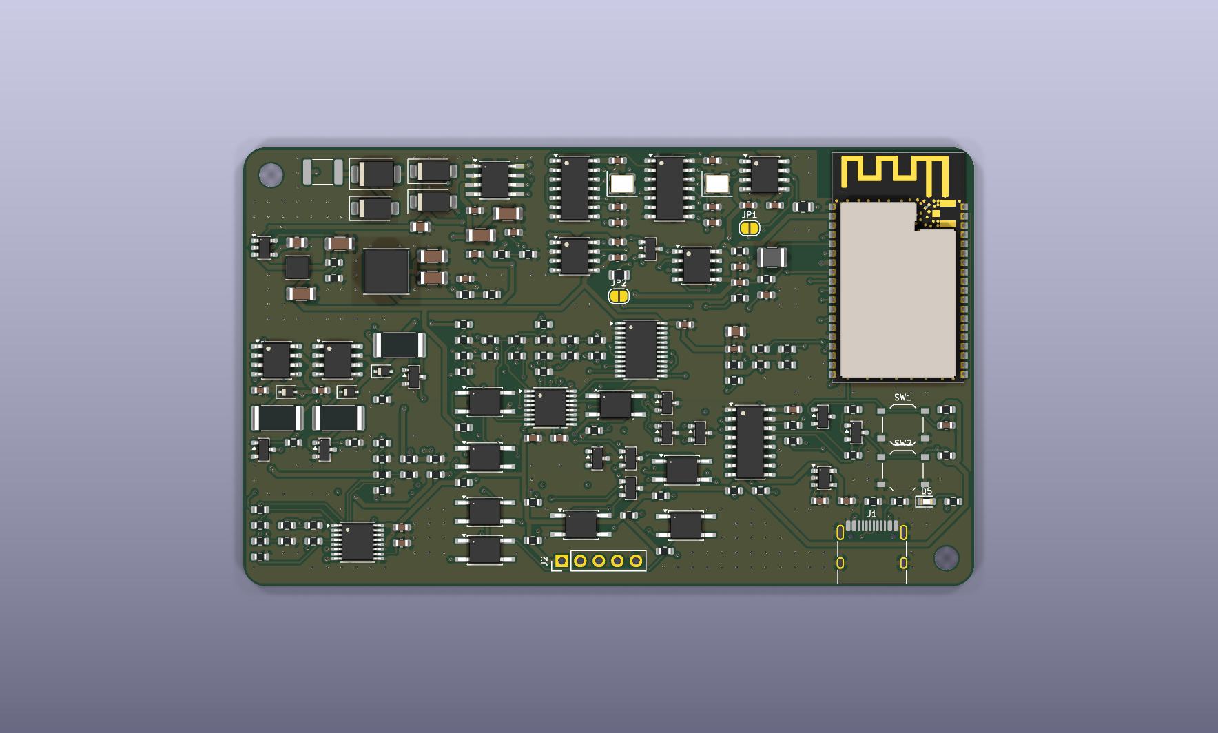
Cyd obd adapter is an open-source printed circuit board by ssjrocks, from the ssjrocks/cyd-obd-adapter repository on GitHub, published under the AGPL-3.0 licence. It is a 4-layer board of 100 × 60 mm with 170 parts on 143 nets, routed with 2,119 tracks and 487 vias.
It is built around the TJA1021T/20/C, TJA1042T/3 and CH340C, with the ESP32-WROVER-E-N8R8, ADS7828E/2K5 and TLV62569DBVR-TP among its other parts. Its parts include 74 resistors, 38 capacitors, 15 ICs, 15 diodes and 10 switches. It belongs with the radio and wireless and interfaces and adapters boards and the ESP32 boards of this library.


An open, low-level OBD-II adapter: an ESP32 with every bus a car's diagnostic port uses, exposed over Bluetooth Classic, BLE, WiFi and USB as a raw proxy. Another device (phone, laptop, the cyd-vehicle-dash screen) sends raw CAN frames and K-line bytes; the adapter puts them on whichever pins the selected car profile uses.
Designed around a 2005 Holden/Opel Astra H, where a cheap ELM327 only reaches the engine ECU: the instrument cluster and body modules sit on single-wire CAN (pin 1) and the gearbox possibly on another line.
Status: schematic and PCB complete (100 × 60 mm, 4 layers, DRC clean), JLCPCB files generated. Nothing built or tested.
| OBD pin(s) | Channel | Hardware |
|---|---|---|
| 6 / 14 | HS-CAN (fixed) | ESP32 TWAI + TJA1042T/3 |
| 1 | Single-wire CAN / GMLAN (33.3 / 83.3 kbit/s) | MCP2518FD + NCV7356 |
| 3/11 or 12/13 | Flex CAN (e.g. Opel MS-CAN, GM chassis HS-CAN) | MCP2518FD + TJA1042T/3, routed by photoMOS switches |
| 7 | K-line 1 (fixed) | TJA1021 + 510 Ω pull-up + MOSFET for slow init |
| 3, 8, 12 or 13 | K-line 2 (routed) | TJA1021 + 510 Ω pull-up + MOSFET |
| 15 | L-line | MOSFET + 510 Ω pull-up |
| all signal pins + battery | Voltage probe | 2× ADS7828, 100k/20k dividers (15 V full scale) |
| 16 / 4, 5 | Battery / grounds | Polyfuse, SMBJ26A TVS, reverse-polarity Schottky |
Nothing connects to the manufacturer-specific pins until the firmware closes a switch. The probe ADCs let the firmware check what is on a pin first: CAN idles at about 2.5 V, a K-line at about 12 V.
J1850 (pins 2/10, older US Fords/GMs) is not implemented; those pins are only measured.
| GPIO | Net | Notes |
|---|---|---|
| 25 / 26 | TWAI_TX / TWAI_RX | HS-CAN; 26 is RTC (wake) |
| 18 / 19 / 23 | SPI SCK / MISO / MOSI | both MCP2518FD |
| 5 / 27 | CS_FCAN / CS_SWCAN | 10k pull-ups |
| 32 / 33 | INT_FCAN / INT_SWCAN | RTC (wake), 10k pull-ups |
| 4 / 36 | K1_TX / K1_RX | UART1; RX has 4.7k pull-up (open-drain TJA1021) |
| 14 / 39 | K2_TX / K2_RX | UART2 |
| 13 | K1_FORCE | MOSFET holds K1 low (slow init); 100k pull-down |
| 12 | K2_FORCE | strap pin, must be low at boot (100k pull-down) |
| 15 | L_DRV | L-line low when high |
| 35 | VBAT_SENSE | 470k/100k: V = adc × 5.7 |
| 34 | AUX_ADC | to J2 |
| 21 / 22 | I2C SDA / SCL | TCA9555 @0x20, ADS7828 @0x48 and @0x49 |
| 2 | LED_STATUS | |
| 0 / EN | BOOT / RESET | buttons + USB auto-reset |
| 1 / 3 | UART0 | CH340C |
Outputs are active low for the switches. At power-up every pin is an input, so all switches are open.
| Pin | Function | Pin | Function |
|---|---|---|---|
| P00 | flex CAN-H → OBD 3 | P10 | HS-CAN STB (high = standby) |
| P01 | flex CAN-L → OBD 11 | P11 | flex CAN STB |
| P02 | flex CAN-H → OBD 12 | P12 | SW-CAN MODE0 |
| P03 | flex CAN-L → OBD 13 | P13 | SW-CAN MODE1 |
| P04 | K2 → OBD 3 | P14 | K1 SLP_N (high = normal) |
| P05 | K2 → OBD 8 | P15 | K2 SLP_N |
| P06 | K2 → OBD 12 | P16, P17 | spare |
| P07 | K2 → OBD 13 |
The firmware must never put two channels on one pin, for example flex CAN-H and K2 both on pin 3.
Volts = code / 4096 × 2.5 × 6.
| ADC | CH0 | CH1 | CH2 | CH3 | CH4 | CH5 | CH6 | CH7 |
|---|---|---|---|---|---|---|---|---|
| 0x48 | OBD1 | OBD2 | OBD3 | OBD6 | OBD7 | OBD8 | OBD9 | OBD10 |
| 0x49 | OBD11 | OBD12 | OBD13 | OBD14 | OBD15 | battery (pin 16) | +5V | VBAT after protection |
hardware/          KiCad 10 project (open cyd-obd-adapter.kicad_pro)
  *.kicad_sch      root + 5 sheets: power, mcu, can, kline, obd
  lib/             project symbols (NCV7356, OBD plug), footprints (OBD plug, ESP32-WROVER-E) and 3D model
  routing/         Freerouting input/output (board.dsn, board.ses)
  production/      JLCPCB files: gerbers.zip, bom_jlcpcb.csv, cpl_jlcpcb.csv
docs/              renders
tools/
  design.py        THE source of the circuit: every part, footprint, LCSC number and connection
  gen_schematic.py builds the schematic sheets from design.py
  check_netlist.py checks a KiCad netlist export against design.py
  make_lib.py      builds the project library
  place.py         board outline, stackup, net classes, planes, component placement
  route.py         export to / import from Freerouting, outer GND pours, stitching vias, zone fill
  fixup.py         finishes leftover connections with a small maze router
  production.sh    exports the JLCPCB fabrication and assembly files
  jlc.py, jlc_exact.py, ds.sh   JLCPCB stock lookup, datasheet download
datasheets/        local copies of datasheets (git-ignored; see links below)
Workflow while the design is changing: edit tools/design.py, then:
python3 tools/gen_schematic.pyCheck the result with kicad-cli sch export netlist and tools/check_netlist.py. Once the PCB is being laid out, edit the schematic in KiCad directly, because regenerating replaces the sheets.
100 × 60 mm, 4 layers:
GND pours on both outer layers are stitched to In1 by about 200 vias.
Routing: fully routed, 0 DRC errors, 0 unconnected.
OBD plug on the bottom, everything else on top. The ESP32 antenna sits at the top edge with a copper keepout under it, so keep metal away from that edge in the enclosure.
Net classes: power 0.6 mm, K-line/L-line 0.4 mm, VBUS 0.4 mm, CAN 0.25 mm, default 0.2 mm.
The board grew from the ~90 × 55 mm target: with 0603 passives and all three regions (power/CAN along the top, K-line and OBD routing in the middle, MCU right) the packer couldn't fit below 100 × 60.
Layout workflow (KiCad closed):
python3 tools/place.py            # re-place from scratch (deletes tracks)
python3 tools/route.py export     # -> hardware/routing/board.dsn, then run Freerouting
python3 tools/route.py import     # board.ses -> board, pours, stitching vias, fill
python3 tools/fixup.py            # routes what Freerouting left (A* on a 0.1 mm grid), loops on KiCad DRC
tools/production.sh               # -> hardware/production/
Freerouting command used (Java 25 required):
java -jar freerouting-2.4.1.jar -de hardware/routing/board.dsn -do hardware/routing/board.ses -mp 40 -mt 4 --gui.enabled=false.
Once you start hand-editing the layout in KiCad, stop using place.py and route.py: they replace the placement and all tracks.
hardware/production/gerbers.zip, then choose: 4 layers, 1.6 mm, 100 × 60 mm.bom_jlcpcb.csv and cpl_jlcpcb.csv.SO-4_4.4x3.6mm_P2.54mm; check it against Panasonic's land pattern.GNU Affero General Public License v3.0.
Exception: hardware/lib/cyd-obd.pretty/ESP32-WROVER-E.kicad_mod and hardware/lib/3d/ESP32-WROVER-E.STEP are copied from Espressif's KiCad libraries and remain under CC-BY-SA 4.0.
| Qty | Value | Footprint | References |
|---|---|---|---|
| 22 | 100k | Resistor_SMD:R_0603_1608Metric | R1, R3, R6, R30, R32, R34, R43, R45, R47, R49, R51, R53, R55, R57, R59, R61 +6 |
| 17 | 100nF | Capacitor_SMD:C_0603_1608Metric | C3, C12, C14, C18, C19, C20, C21, C24, C25, C26, C29, C32, C33, C34, C35, C37 +1 |
| 16 | 20k | Resistor_SMD:R_0603_1608Metric | R44, R46, R48, R50, R52, R54, R56, R58, R60, R62, R64, R66, R68, R70, R72, R74 |
| 8 | 10k | Resistor_SMD:R_0603_1608Metric | R7, R8, R9, R10, R11, R12, R22, R23 |
| 8 | 390 | Resistor_SMD:R_0603_1608Metric | R35, R36, R37, R38, R39, R40, R41, R42 |
| 8 | AQY282SX | Package_SO:SO-4_4.4x3.6mm_P2.54mm | K1, K2, K3, K4, K5, K6, K7, K8 |
| 7 | NUP2105L | Package_TO_SOT_SMD:SOT-23 | D6, D10, D11, D12, D13, D14, D15 |
| 6 | 1uF | Capacitor_SMD:C_0603_1608Metric | C4, C15, C16, C17, C36, C38 |
| 6 | 4.7k | Resistor_SMD:R_0603_1608Metric | R13, R14, R15, R16, R20, R21 |
| 4 | 22pF | Capacitor_SMD:C_0603_1608Metric | C22, C23, C27, C28 |
| 4 | 22uF 25V | Capacitor_SMD:C_1206_3216Metric | C6, C7, C10, C11 |
| 3 | 10uF 25V | Capacitor_SMD:C_0805_2012Metric | C8, C9, C13 |
| 3 | 1N4148WS | Diode_SMD:D_SOD-323 | D7, D8, D9 |
| 3 | 2N7002 | Package_TO_SOT_SMD:SOT-23 | Q3, Q4, Q5 |
| 3 | 510 1W | Resistor_SMD:R_2512_6332Metric | R29, R31, R33 |
| 2 | 100pF | Capacitor_SMD:C_0603_1608Metric | C30, C31 |
| 2 | 120 | Resistor_SMD:R_0805_2012Metric | R24, R25 |
| 2 | 1k | Resistor_SMD:R_0603_1608Metric | R17, R28 |
| 2 | 2.2uF 50V | Capacitor_SMD:C_1206_3216Metric | C1, C2 |
| 2 | 40MHz | Crystal:Crystal_SMD_3225-4Pin_3.2x2.5mm | Y1, Y2 |
| 2 | 5.1k | Resistor_SMD:R_0603_1608Metric | R18, R19 |
| 2 | ADS7828E/2K5 | Package_SO:TSSOP-16_4.4x5mm_P0.65mm | U14, U15 |
| 2 | M3 | MountingHole:MountingHole_3.2mm_M3 | H1, H2 |
| 2 | MCP2518FDT-E/SL | Package_SO:SOIC-14_3.9x8.7mm_P1.27mm | U7, U9 |
| 2 | MMBT3904 | Package_TO_SOT_SMD:SOT-23 | Q1, Q2 |
| 2 | SS14 | Diode_SMD:D_SMA | D3, D4 |
| 2 | TJA1021T/20 | Package_SO:SOIC-8_3.9x4.9mm_P1.27mm | U11, U12 |
| 2 | TJA1042T/3 | Package_SO:SOIC-8_3.9x4.9mm_P1.27mm | U6, U8 |
| 1 | 0.75A/33V | Fuse:Fuse_1812_4532Metric | F1 |
| 1 | 2.2uH | Inductor_SMD:L_Sunlord_SWPA3015S | L2 |
| 1 | 2.7k | Resistor_SMD:R_0603_1608Metric | R26 |
| 1 | 22k | Resistor_SMD:R_0603_1608Metric | R4 |
| 1 | 22uH | Inductor_SMD:L_Sunlord_SWPA6045S | L1 |
| 1 | 24k | Resistor_SMD:R_0603_1608Metric | R2 |
| 1 | 470k | Resistor_SMD:R_0603_1608Metric | R5 |
| 1 | 47uH | Inductor_SMD:L_1210_3225Metric | L3 |
| 1 | 6.49k | Resistor_SMD:R_0603_1608Metric | R27 |
| 1 | AP2112K-3.3TRG1 | Package_TO_SOT_SMD:SOT-23-5 | U4 |
| 1 | AUX | Connector_PinHeader_2.54mm:PinHeader_1x05_P2.54mm_Vertical | J2 |
| 1 | BOOT | Button_Switch_SMD:SW_Push_1P1T_XKB_TS-1187A | SW2 |
| 1 | CH340C | Package_SO:SOIC-16_3.9x9.9mm_P1.27mm | U5 |
| 1 | ESP32-WROVER-E-N8R8 | cyd-obd:ESP32-WROVER-E | U3 |
| 1 | FCAN_TERM | Jumper:SolderJumper-2_P1.3mm_Open_RoundedPad1.0x1.5mm | JP2 |
| 1 | HS_TERM | Jumper:SolderJumper-2_P1.3mm_Open_RoundedPad1.0x1.5mm | JP1 |
| 1 | LMR36510ADDAR | Package_SO:Texas_HTSOP-8-1EP_3.9x4.9mm_P1.27mm_EP2.95x4.9mm_Mask2.4x3.1mm_ThermalVias | U1 |
| 1 | NCV7356D1R2G | Package_SO:SOIC-8_3.9x4.9mm_P1.27mm | U10 |
| 1 | OBD-FMB-16-SN-B-E-R-V2 | cyd-obd:OBD2_Male_Antenk_OBD-FMB-16_SMD | J3 |
| 1 | RESET | Button_Switch_SMD:SW_Push_1P1T_XKB_TS-1187A | SW1 |
| 1 | SMBJ26A | Diode_SMD:D_SMB | D1 |
| 1 | SS210 | Diode_SMD:D_SMA | D2 |
| 1 | TCA9555PWR | Package_SO:TSSOP-24_4.4x7.8mm_P0.65mm | U13 |
| 1 | TLV62569DBVR | Package_TO_SOT_SMD:SOT-23-5 | U2 |
| 1 | USB-C | Connector_USB:USB_C_Receptacle_HRO_TYPE-C-31-M-12 | J1 |
| 1 | red | LED_SMD:LED_0603_1608Metric | D5 |


snhobbs/scopefun-hardware
This repository contains Scopefun hardware schematics and pcb layout files.

jlcjak/astra_piNas
Six-layer CM5 Lite dual-NVMe carrier with PCIe switch, Ethernet, microSD, USB-C PD and PoE. Review design; fabrication hold documented.


It measures 100 × 60 mm and has 4 copper layers, 1.6 mm thick.
170 parts, built around the TJA1021T/20/C, TJA1042T/3, CH340C and ESP32-WROVER-E-N8R8. The full list of its parts is on this page, with links to each part's symbol and footprint where PCBKit's library has them.
From the ssjrocks/cyd-obd-adapter repository on GitHub, at the commit this page was made from: the board is hardware/cyd-obd-adapter.kicad_pcb and its schematic hardware/can.kicad_sch. PCBKit opens the board in the browser, with nothing to install.
Its repository publishes it under the AGPL-3.0 licence: you may reuse it on that licence's terms (keep the author's notice, and for a copyleft licence share your changes alike).