2 layers71.1 × 71.1 mm

 speedypleath/wheel-module-kicad
PCB for wheel module
Haptic console wheel module stripboard is an open-source printed circuit board by speedypleath, from the speedypleath/wheel-module-kicad repository on GitHub. It is a 2-layer board of 104.1 × 104.1 mm with 21 parts on 39 nets, routed with 92 tracks and 1,331 vias.
Its parts include 6 resistors, 2 capacitors, 2 diodes, 2 connectors and 1 IC. It belongs with the RP2040 boards of this library.
KiCad project for the electronics of the Wheel Module (M3) of Haptic Console v1.0, part of the ITPMA dissertation Tactile I/O: Exploring physicality in MIDI controllers.
The mechanical side of this module (200 mm DIN aluminium handwheel, PETG shaft,
6204-2RS bearings, GT2 1:1 belt drive) is documented in the Obsidian vault under
Notes/Haptic Console - Handwheel Belt Drive Module Plan.md. This repository covers
only the sensor board that reads the optical encoder and presents it to the console.
The handwheel drives an E38S6G5-600B-G24N 600 P/R optical encoder through a 1:1 GT2 belt. A Raspberry Pi Pico reads the A/B quadrature signals locally, converts them into a clean position packet, and exposes that packet to the Teensy 4.1 master over I2C. The module behaves as a self-contained tactile sense organ rather than a peer processor, matching the connector standard's design philosophy.
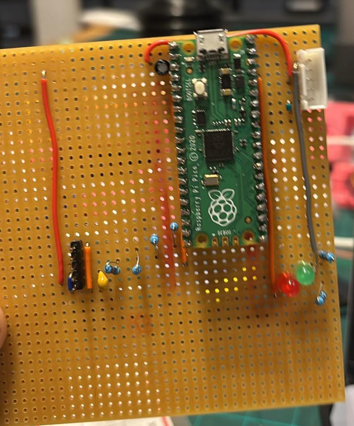
The module as actually built. Component side, left to right: J2 (black 5-pin encoder
header) and the pull-up/series resistors bottom left, C2 (yellow disc) beside them,
U1 centre with C1's electrolytic can at its USB end, J1 (white XH2.54 to the hub)
top right, and the D1/D2 status LEDs bottom right.
The encoder is an E38S6G5-600B-G24N: photoelectric incremental, 600 P/R, rated
DC 5-24V, with NPN open-collector outputs. The 600B suffix denotes AB
two-phase — there is no Z index channel. Absolute zero is established in firmware,
not from hardware index.
The open-collector output is the important electrical detail. An open-collector output can only pull its line low. It never drives a line high. The high level is therefore set entirely by whatever rail the line is pulled up to, and is completely independent of the encoder's own supply voltage.
That gives the safety property this board relies on:
R1, R2 (4.7k) pull ENC_A_RAW and ENC_B_RAW up to +3V3.R4, R5 (330R) sit in series into the Pico GPIO as fault-current limiters,
protecting the pin if a line is ever accidentally shorted to the encoder supply.4.7k is comfortable here. With ~2 m of encoder cable at roughly 120 pF/m plus pin and stray capacitance (~300 pF total), the RC rise time is about 3 us 10-90%. At a realistic handwheel speed of 300 rev/min each channel runs at 3 kHz, a 333 us period, so the rise occupies under 1% of it. Pull-up current is 0.7 mA per line, far inside the output stage's sink capability.
Without the pull-ups the inputs would float and the quadrature decode would be noise. The pull-ups are not optional here.
Encoder power is taken from the console's 5V rail, which is inside the encoder's
rated 5-24V window. If the encoder proves sluggish or noisy at 5V, the documented
alternative is a small 5V to 12V boost feeding J2 pin 1 only. Because the pull-ups
reference 3.3V, that change requires no modification to the logic side.
Decision, 2026-08-28: the 12V path is deliberately not built. The planned Eurorack translation module needs 24V regardless, so if a higher-voltage rail is ever added it should be designed once for both modules rather than bolted onto M3 alone. Treat 5V as the committed supply until that point. Note also that if the encoder signals ever look sluggish, supply voltage is the less likely cause: edge shape here is set by the pull-up RC (4.7k against ~300 pF, ~3 us) which does not change with encoder supply at all. Rounded edges point at the pull-ups (fit 2.2k or 1k); missed counts that worsen with rotation speed point at the supply.
J1 is the standard XH2.54 6-pin inter-module connector (standard v1.1):
| Pin | Signal | Board use |
|---|---|---|
| 1 | GND | Common ground |
| 2 | 3.3V | Not connected (see below) |
| 3 | 5V | Powers the Pico via VSYS, and the encoder |
| 4 | SIG1 / SDA | I2C data, Pico GP4 |
| 5 | SIG2 / SCL | I2C clock, Pico GP5 |
| 6 | SIG3 / IRQ | Data-ready, Pico GP6 |
Pin 2 is deliberately left unconnected. The connector standard warns against feeding both VSYS and 3V3 as competing power paths into a Pico. The board takes 5V into VSYS and uses the Pico's own regulated 3V3 output as the logic reference for the pull-ups.
I2C bus pull-ups live on the master/hub board, not here, per the same standard.
J2 is a 5-pin 2.54mm header matching the encoder's four conductors plus its shield:
| Pin | Encoder wire | Board use |
|---|---|---|
| 1 | Red | V+, from the console 5V rail |
| 2 | Black | 0V / GND |
| 3 | White | Channel A, to R1/R4 |
| 4 | Green | Channel B, to R2/R5 |
| 5 | Bare / foil | Cable shield, to GND |
Pin 5 carried ENC_Z in the first revision. The encoder has no Z channel, so it is now
the shield return, terminated to GND at the board end only — single-point, to avoid
a ground loop down the 2 m cable run.
| Pico pin | Net | Function |
|---|---|---|
| GP2 (pin 4) | LNK | Link/comms status LED |
| GP4 (pin 6) | SDA | I2C target data |
| GP5 (pin 7) | SCL | I2C target clock |
| GP6 (pin 9) | IRQ | Data-ready out to master |
| GP16 (pin 21) | ENC_A | Encoder channel A |
| GP17 (pin 22) | ENC_B | Encoder channel B |
| VSYS (pin 39) | +5V | Module power in |
| 3V3 (pin 36) | +3V3 | Logic reference out |
At 600 P/R with 4x quadrature decoding, one full handwheel turn is 2400 counts.
C1 is a bulk reservoir, not a decoupling capacitor, and the two jobs are different. C2 (100 nF on 3V3) is decoupling: it kills the nanosecond-scale current spikes from GPIO switching, and wants to be small and close to the pin. C1 sits on the 5 V rail at the connector entry and does the opposite job — it is a local charge store at the far end of the hub cable.
The 5 V arrives over a metre or two of XH2.54 flying lead, perhaps 1 uH/m of inductance plus some milliohms. Every change in this board's load current has to be supplied through that inductance: the encoder's output transistors switching at 2 x 3 kHz, the Pico's RT6150 buck-boost drawing pulsed input current, and above all hot-plugging J2 with the encoder attached. Without local bulk the rail at VSYS dips and rings instead of holding up. Steady-state draw is modest — encoder 40-100 mA, Pico 25-30 mA, LEDs ~3 mA — so it is the transients that matter.
100 nF will not do this job: it is 100x less charge. A 100 mA step lasting 300 ns gives dV = I*dt/C ~= 300 mV on 100 nF against ~3 mV on 10 uF, and it moves the cable-inductance resonance from ~50 kHz up to ~500 kHz where it is far less damped.
Electrolytic is the right part, not a compromise — bulk capacitance is what
aluminium electrolytics are for. The first revision specified a 10 uF ceramic only
because Device:CP cached as a zero-pin stub during project creation and switching
to the non-polarised Device:C sidestepped the question. (The real cause was
simpler: KiCad 10 has no Device:CP at all; the symbol is Device:C_Polarized.)
C1 is now polarised, and nothing in ERC or DRC will catch it if you fit it
backwards. Pad 1 is + and goes to +5V; the lead beside the printed stripe is
- and goes to GND. On a 5 V rail a reversed electrolytic will vent. Both build
guides call this out at the step where it matters.
| Ref | Value | Footprint |
|---|---|---|
| U1 | Raspberry Pi Pico | Module:RaspberryPi_Pico_Common_THT |
| J1 | XH2.54 6-pin console connector | Connector_JST:JST_XH_B6B-XH-A_1x06_P2.50mm_Vertical |
| J2 | 5-pin encoder header | Connector_PinHeader_2.54mm:PinHeader_1x05_P2.54mm_Vertical |
| R1, R2 | 4.7k pull-up to 3.3V | Resistor_THT:R_Axial_DIN0207_L6.3mm_D2.5mm_P10.16mm_Horizontal |
| R4, R5 | 330R series protection | Resistor_THT:R_Axial_DIN0207_L6.3mm_D2.5mm_P10.16mm_Horizontal |
| R7, R8 | 1k LED current limit | Resistor_THT:R_Axial_DIN0207_L6.3mm_D2.5mm_P10.16mm_Horizontal |
| C1 | 10uF 25V bulk on 5V, polarised | wheel-module:CP_Radial_D4.0mm_P2.50mm |
| C2 | 100nF decoupling on 3.3V | Capacitor_THT:C_Disc_D5.0mm_W2.5mm_P5.00mm |
| D1 | PWR green 3mm | LED_THT:LED_D3.0mm |
| D2 | LNK red 3mm | LED_THT:LED_D3.0mm |
D1 and D2 match the PWR/LNK status cluster in the front panel drawing
(Notes/Haptic Console - Wheel Module Front Panel.md).
One schematic, three board files. They share the netlist and nothing else — pick the one that matches how you are building.
| Build | Board file | Build guide |
|---|---|---|
| Stripboard (Veroboard) | project/haptic-console-wheel-module-stripboard.kicad_pcb | docs/stripboard-wiring.md, or the interactive docs/stripboard-wiring.html with a live board map |
| Plain perfboard | project/haptic-console-wheel-module-perfboard.kicad_pcb | docs/perfboard-wiring.md |
| Fabricated PCB | project/haptic-console-wheel-module.kicad_pcb | none needed — Gerber set |
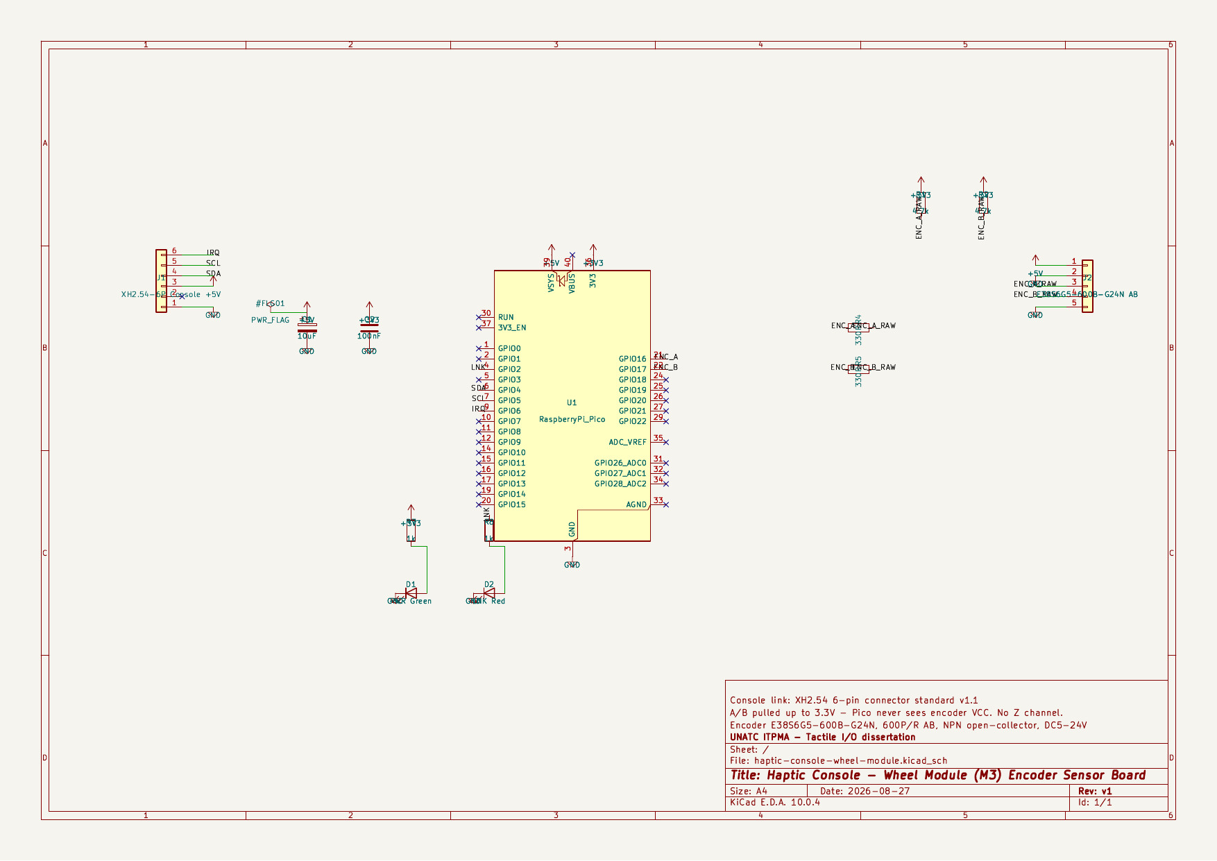
Full page as renders/schematic-v2.pdf. ERC report:
docs/erc-report.txt; exported netlist:
docs/netlist.net.
40 x 40 holes, 104.14 mm square — the full uncut board. The circuit lives in cols 1-28 / rows 1-28; the strips run the board's whole width regardless, which is why the audit matters more than the placement.
| Component side | Solder side |
|---|---|
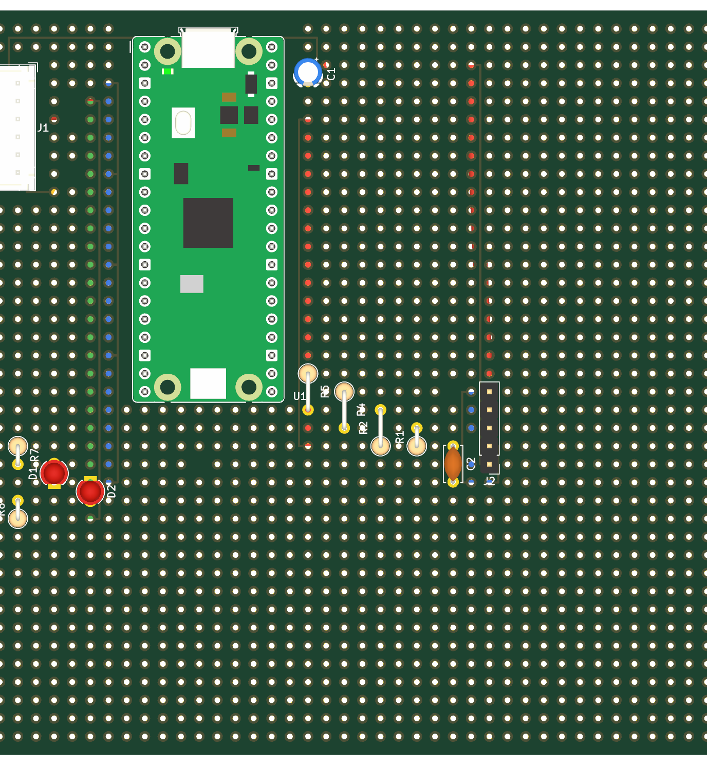 | 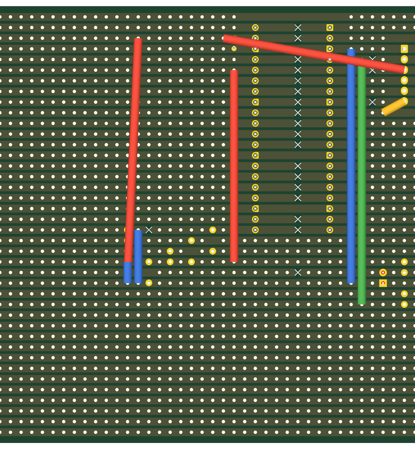 |
The solder-side view is the one to build from: white X marks are the 23 track cuts, and
the coloured rods are the eight link wires, drawn to the control unit's colour convention
(red power, blue GND, yellow I2C/IRQ, green /LNK). Cuts and links are listed
step-by-step in docs/stripboard-wiring.md.
28 x 28 holes, 71.12 mm square, every connection a discrete wire.
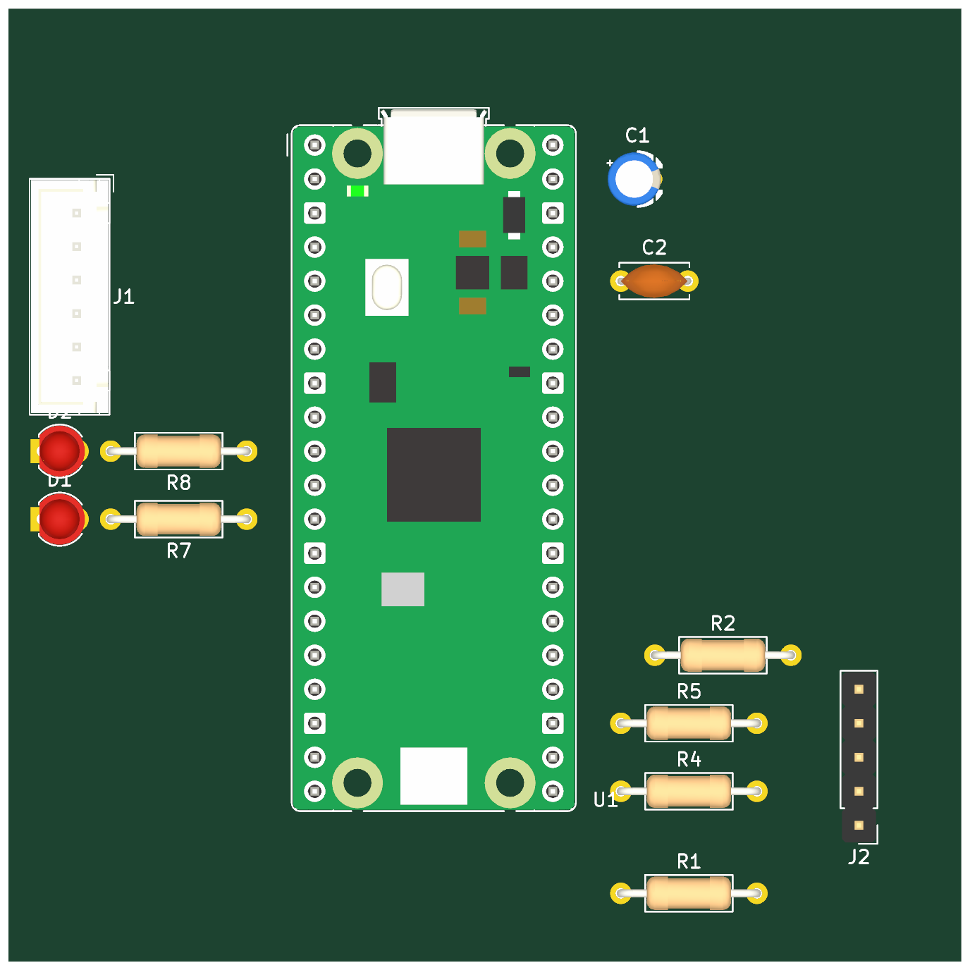
Wire-by-wire build order in docs/perfboard-wiring.md.
68 x 58 mm, 2-layer, all through-hole.
| Front (F.Cu) | Back (B.Cu) |
|---|---|
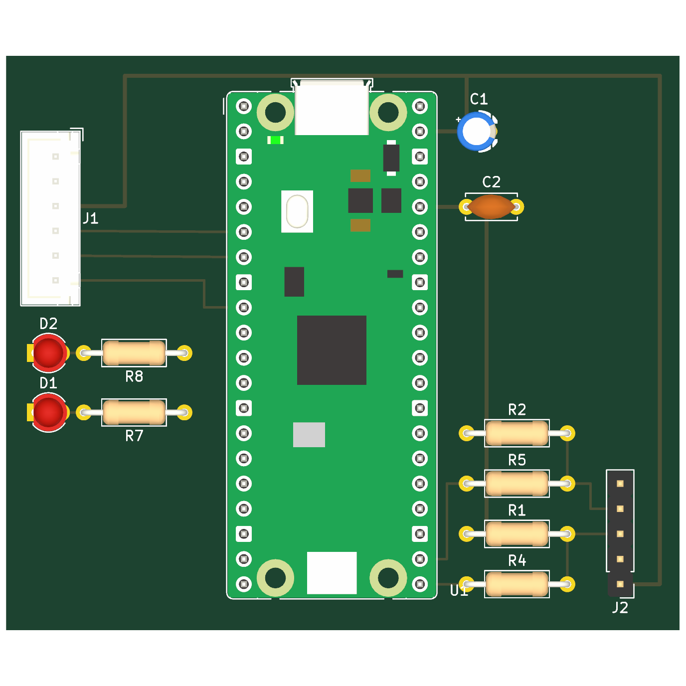 | 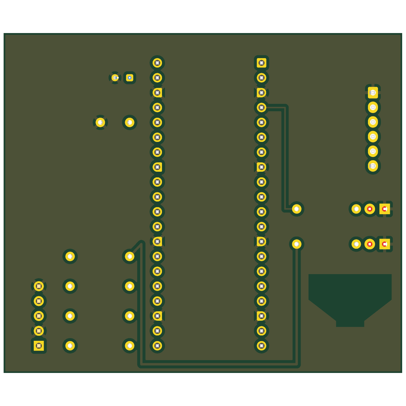 |
The back is mostly the filled GND pour that all 14 GND pads tie into; only /LNK and the
+3V3 branch to R7 are routed there.
docs/netlist.net — 13 components, 15 nets, every node checked against the
pin map above. A clean ERC alone does not prove connectivity; always read the netlist.ENC_Z, R3 and R6 removed after the datasheet confirmed the
600B part is AB two-phase. J2 pin 5 repurposed as shield. GP18 is now free.J1 pin 2
(hub 3.3V) unconnected. Rows 4/14/19 are left uncut on purpose - they carry GND on
both sides of the Pico and form the GND bus for free. The ~240 DRC warnings are
expected: perfboard holes modelled as vias dangle by construction.
Generated from scripts/layout.py by the shared ~/KiCad/kicad-stripboard
engine - rebuild it rather than editing the board.
The eight physical link wires are modelled as colour-coded 3D jumper wires on the
solder side, keeping the crowded component side clear.B.Cu (3270 mm² of copper), which all 14 GND pads
tie into directly, so GND needs no traces. Two runs sit on the back layer because they would otherwise cross the J1 signal fan
on the front: /LNK (U1.4 → R8.1) and the +3V3 branch feeding R7, which goes round
the bottom at y=56.5 rather than threading the 0.94 mm gaps between the Pico's pad
rows. The front +3V3 spine is offset to x=48.5 rather than running down the x=46.5
pad column, because R5.1 (/ENC_B) sits mid-column at 46.5,43.18.export KICAD_SYMBOL_DIR=/Applications/KiCad/KiCad.app/Contents/SharedSupport/symbols
export KICAD_FOOTPRINT_DIR=/Applications/KiCad/KiCad.app/Contents/SharedSupport/footprints
kicad-cli sch erc --format report project/haptic-console-wheel-module.kicad_sch -o docs/erc-report.txt
kicad-cli sch export netlist --format kicadsexpr project/haptic-console-wheel-module.kicad_sch -o docs/netlist.netSetting both environment variables matters. Without them kicad-cli cannot resolve the
stock libraries and reports spurious violations.
docs/perfboard-wiring.md - hand-wiring guide for the
plain-perfboard builddocs/stripboard-wiring.md - cut/link build guide for the
Veroboard build, plus the interactive
docs/stripboard-wiring.htmlscripts/layout.py - the stripboard layout as data; source of
truth for that board../kicad-stripboard - the shared engine that builds and audits strip board layouts../control-unit-kicad - the Control Unit (M6) board, already fab-readyNotes/Haptic Console - Connector Standard.mdconcepts/haptic-console-wheel-module.md| Qty | Value | Footprint | References |
|---|---|---|---|
| 3 | GND | W6, W7, W8 | |
| 2 | +5V | W1, W3 | |
| 2 | 1k | R_Axial_DIN0207_L6.3mm_D2.5mm_P2.54mm_Vertical | R7, R8 |
| 2 | 330R | R_Axial_DIN0207_L6.3mm_D2.5mm_P5.08mm_Vertical | R4, R5 |
| 1 | +3V3 | W4 | |
| 1 | /IRQ | W2 | |
| 1 | /LNK | W5 | |
| 1 | 100nF | C_Disc_D5.0mm_W2.5mm_P5.00mm | C2 |
| 1 | 10uF | CP_Radial_D4.0mm_P2.50mm | C1 |
| 1 | 4.7k | R_Axial_DIN0207_L6.3mm_D2.5mm_P5.08mm_Vertical | R2 |
| 1 | 4.7k | R_Axial_DIN0207_L6.3mm_D2.5mm_P2.54mm_Vertical | R1 |
| 1 | E38S6G5-600B-G24N AB | Connector_PinHeader_2.54mm:PinHeader_1x05_P2.54mm_Vertical | J2 |
| 1 | LNK Red | LED_THT:LED_D3.0mm | D2 |
| 1 | PWR Green | LED_THT:LED_D3.0mm | D1 |
| 1 | RaspberryPi_Pico | Module:RaspberryPi_Pico_Common_THT | U1 |
| 1 | XH2.54-6P Console | Connector_JST:JST_XH_B6B-XH-A_1x06_P2.50mm_Vertical | J1 |

gusmanb/logicanalyzer
24 channel, 100Msps logic analyzer hardware and software

mntmn/amiga2000-gfxcard
MNT VA2000, an Open Source Amiga 2/3/4000 Graphics Card (Zorro II/III), written in Verilog


hackclub/OnBoard
💡 Join 1,000 teenagers and make your first PCB with a $100 grant!

drandyhaas/KiCadRoutingTools
A set of Python/Rust tools to aid routing in KiCad

Arrow-air/project-quiver
Project Quiver documentation, designs, and project artifacts.


It measures 104.1 × 104.1 mm and has 2 copper layers, 1.6 mm thick.
21 parts. The full list of its parts is on this page, with links to each part's symbol and footprint where PCBKit's library has them.
From the speedypleath/wheel-module-kicad repository on GitHub, at the commit this page was made from: the board is project/haptic-console-wheel-module-stripboard.kicad_pcb and its schematic project/haptic-console-wheel-module.kicad_sch. PCBKit opens the board in the browser, with nothing to install.
Its repository states no licence, so its author keeps all rights: ask speedypleath before reusing the design.