2 layers97.2 × 59.1 mm
ArmLEDsPrototype
hackclub/OnBoard
💡 Join 1,000 teenagers and make your first PCB with a $100 grant!
35 parts915

 speedypleath/control-unit-kicad
KiCad project for the Control Unit module of the Haptic Console v1.0. One schematic, two PCBs: a compact manufactured board (SMD, routed, ready for fab) and a hand-wireable perfboard build.
Haptic console control unit is an open-source printed circuit board by speedypleath, from the speedypleath/control-unit-kicad repository on GitHub. It is a 2-layer board of 88 × 131 mm with 35 parts on 50 nets, routed with 654 tracks and 35 vias.
Its parts include 7 resistors, 6 switches, 2 connectors and 1 IC.
KiCad project for the Control Unit module of the Haptic Console v1.0. One schematic, two PCBs: a compact manufactured board (SMD, routed, ready for fab) and a hand-wireable perfboard build.
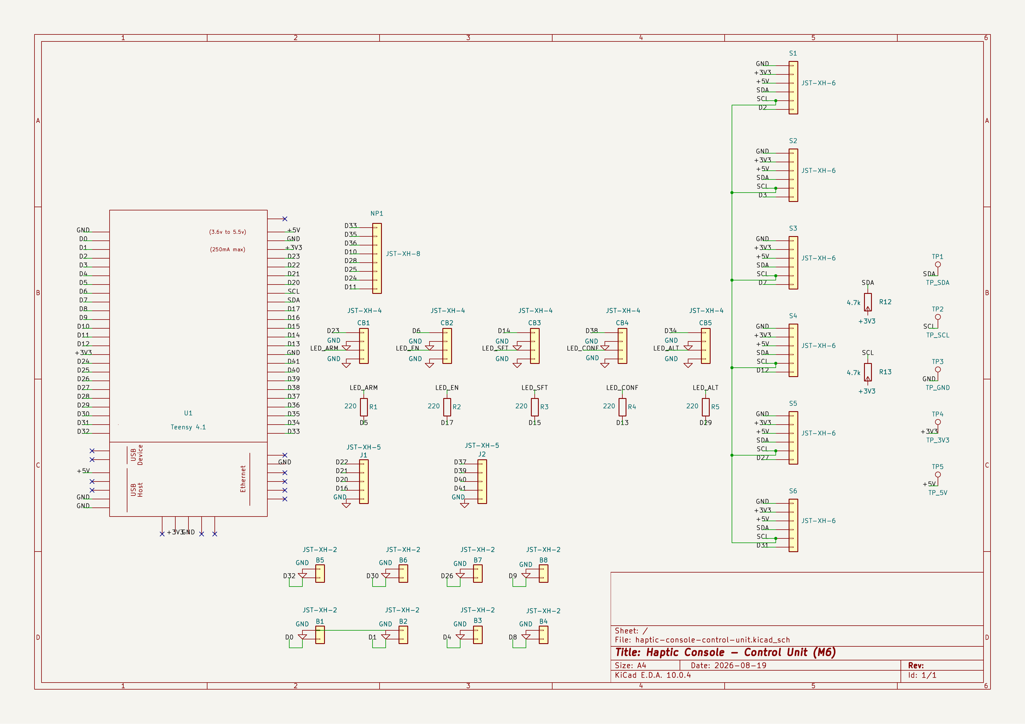
U1 Teensy 4.1, S1–S6 haptic driver connectors (6-pin JST-XH, XH2.54 v1.1 standard), B1–B8 tactile buttons, CB1–CB5 + R1–R5 LED/button conditioning, R12/R13 I²C pull-ups, J1/J2 joystick headers, NP1 numpad matrix, TP1–TP5 test points (SDA/SCL/GND/+3V3/+5V, tapped at the I²C pull-up network). ERC: 0 errors/0 warnings.
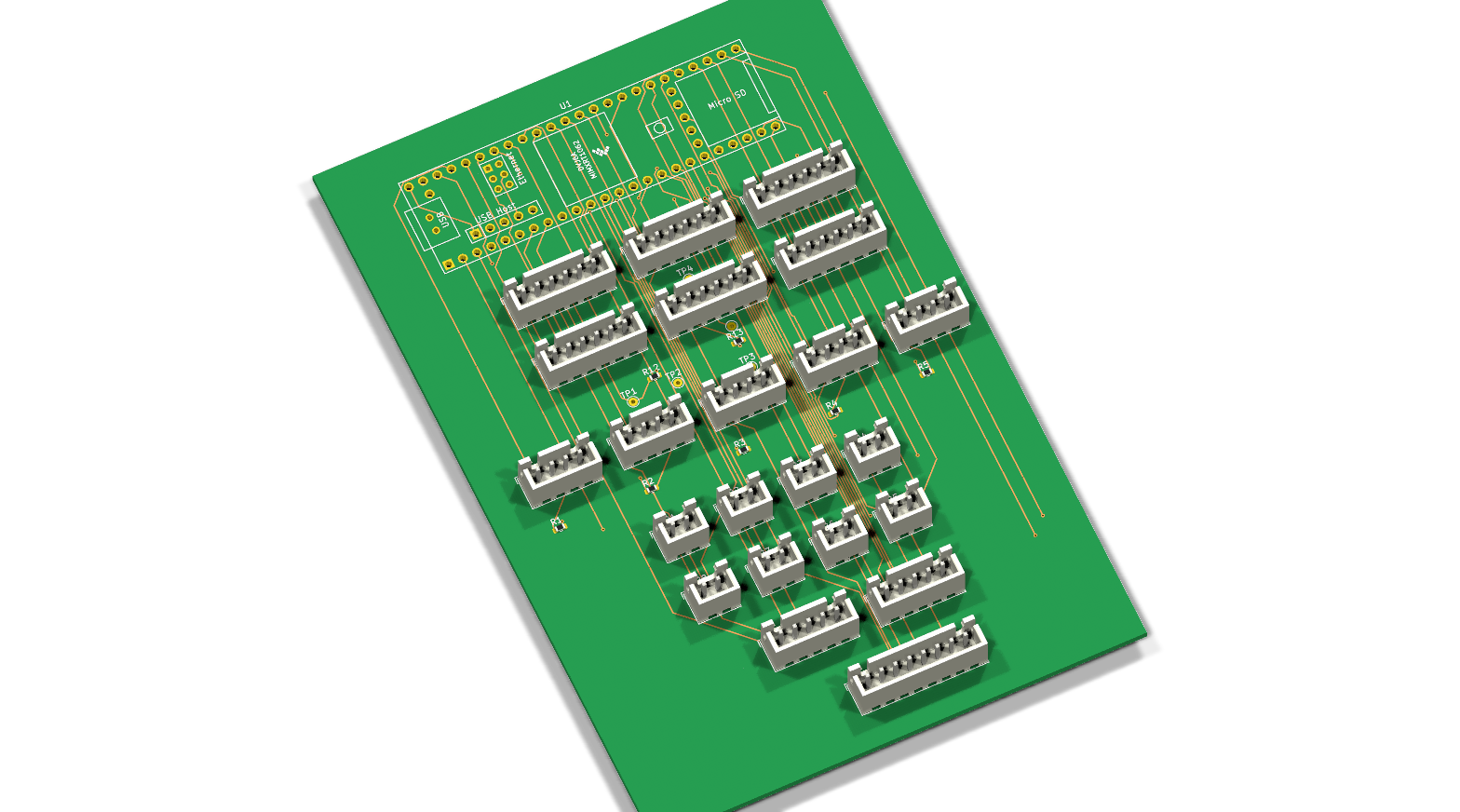
Compact (88×131mm) layout, SMD 0603 resistors, fully autorouted (654 track segments, 35 vias, 0 unrouted nets), plus 5 THT test-point pads (TP1–TP5) for SDA/SCL/GND/+3V3/+5V near R12/R13. DRC: 0 errors/0 warnings, 0 unconnected pads.
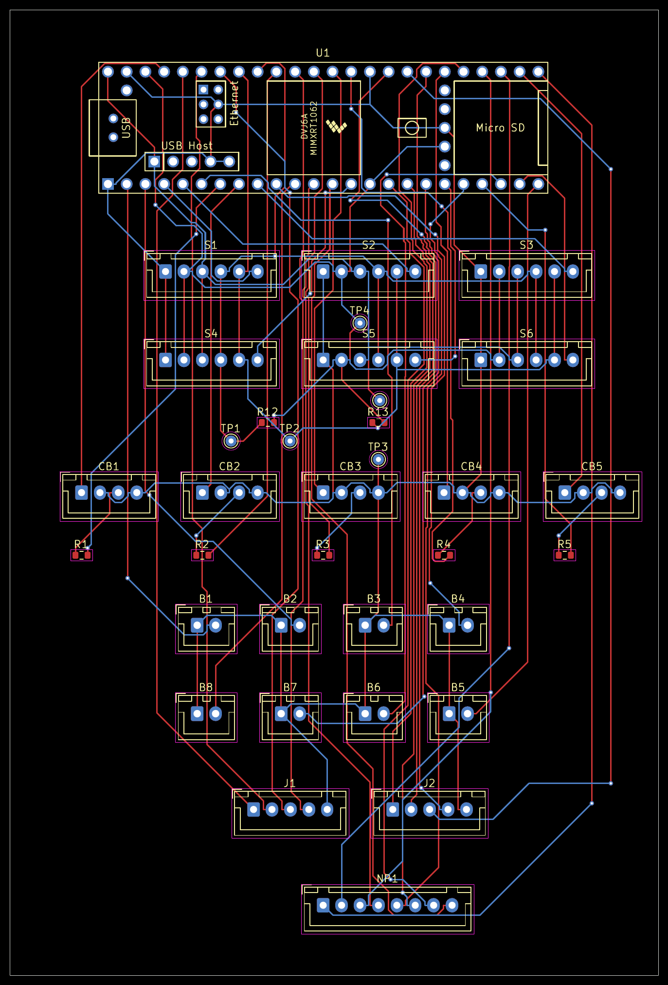
Gerbers + drill file: project/haptic-console-control-unit-gerbers.zip
(Gerber X2 + Excellon drill, plain KiCad-default output — no fab-specific renaming).
View with gerbv or unzip and drag into your fab's order-check
tool (JLCPCB/PCBWay/OSH Park all accept the zip directly).
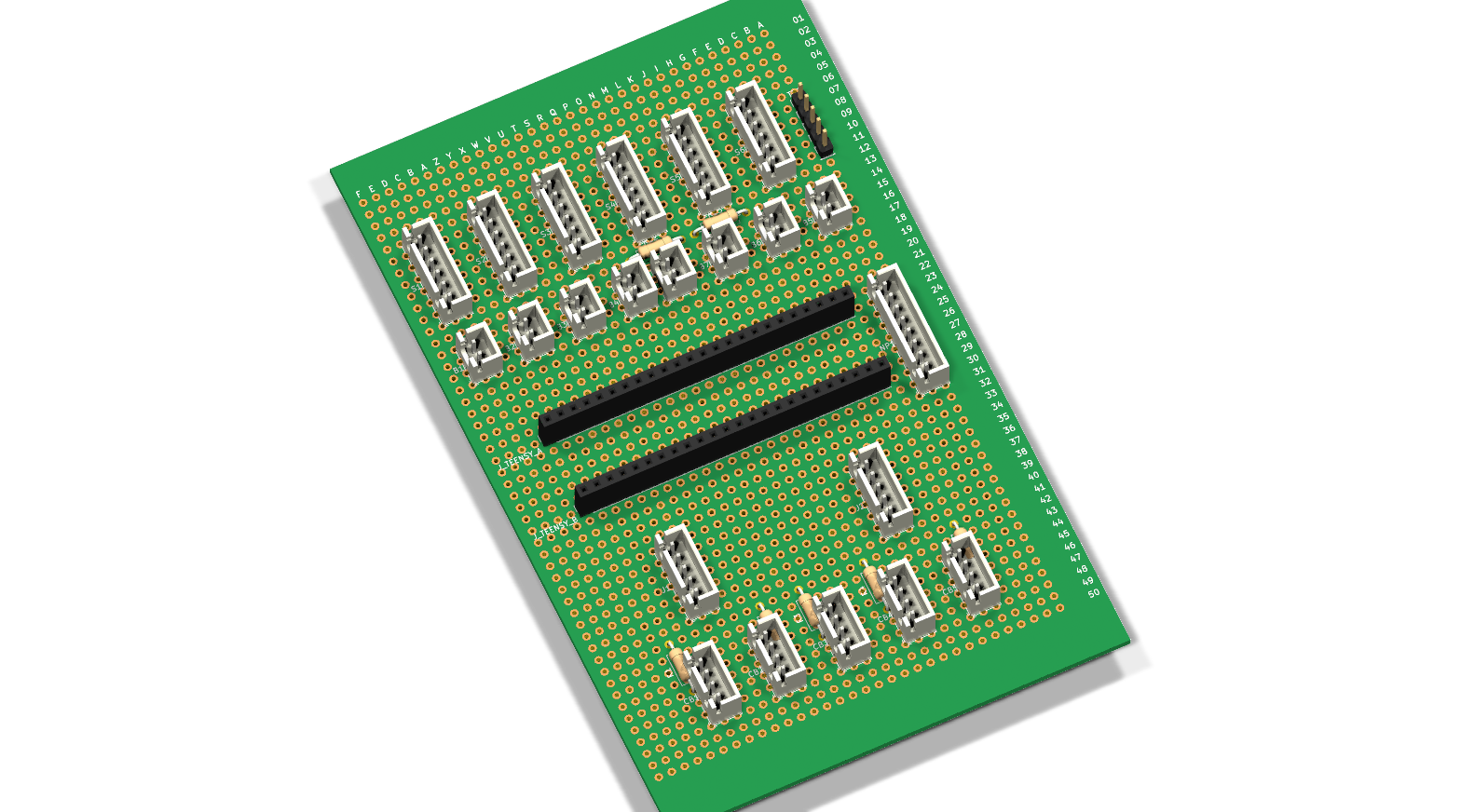
Hand-wireable 90×150mm 32×50-hole perfboard layout, same schematic/nets, laid out for
row/column GND+3V3+5V+SDA+SCL bus wiring, with 223 colour-coded back-side jumper wires
modelled in 3D (see docs/perfboard-wiring-regeneration.md). TP1–TP5 are real male 2.54mm header pins
(not just pads) in the last column at the board's right edge, past S6 — clip a jumper
or scope hook straight on instead of back-probing a live JST connector. Full
per-connector wiring plan (every connection as a board grid reference, e.g.
S1.1 → Q23), live at
wiring-guide
(source: docs/wiring-guide.html). Print
renders/perfboard-placement-template-1to1.pdf
at 100%/Actual Size for physical placement.
Every connector signal is wired to whichever Teensy digital pin sits physically closest
to it, rather than to a contiguous block per function — 1356 mm of Manhattan run in total,
longest single wire 61 mm, 223 modelled jumper legs on the perfboard. The assignments are
therefore not sequential; the authoritative map is scripts/pin_map.json, rendered per
connector in the wiring guide and the
panel wiring guide. Firmware pin constants must follow
that map.
Eighteen conductors are frozen because they are already soldered on the built board and
are an input to the solver, not a result: B1–B8, both joysticks (J1/J2), and the LED4/LED5
lamp jumpers. Everything else — the six module IRQs, the five control-button switches, the
other three lamps and the eight numpad lines — is re-solved for proximity whenever the
layout moves. The Teensy plugs in USB toward the B23/B29 end; if that is ever in
doubt, settle it by reading a hole off the physical board, never by checking whether the
resulting map looks sensible.
S1–S6 haptic-module cables follow XH2.54 6-pin — Haptic Console Connector Standard v1.1: pin 1 GND, pin 2 3.3V, pin 3 5V, pin 4 SDA, pin 5 SCL, pin 6 IRQ.
teensy.pretty / teensy.kicad_sym — XenGi Teensy 4.1 footprint + symbol (not stock
KiCad), vendored in libraries/.Connector_JST, Resistor_THT, Resistor_SMD, Device, Connector_Generic, power
— stock KiCad 10 libraries.digikey-kicad-library, SparkFun-KiCad-Libraries — additional atomic parts.fp-lib-table / sym-lib-table wired for all of the above.project/ — schematic, both boards, project files, lib tables, gerbers/ +
*-gerbers.zip (manufactured board fab output)libraries/ — vendored XenGi teensy.prettyrenders/ — schematic + PCB rendersdocs/ — wiring guide, build log, kicad-mcp lessons| Qty | Value | Footprint | References |
|---|---|---|---|
| 8 | JST-XH-2 | Connector_JST:JST_XH_B2B-XH-A_1x02_P2.50mm_Vertical | B1, B2, B3, B4, B5, B6, B7, B8 |
| 6 | JST-XH-6 | JST_XH_B6B-XH-A_1x06_P2.50mm_Vertical | S1, S2, S3, S4, S5, S6 |
| 5 | 220 | R_0603_1608Metric | R1, R2, R3, R4, R5 |
| 5 | JST-XH-4 | Connector_JST:JST_XH_B4B-XH-A_1x04_P2.50mm_Vertical | CB1, CB2, CB3, CB4, CB5 |
| 2 | 4.7k | R_0603_1608Metric | R12, R13 |
| 2 | JST-XH-5 | Connector_JST:JST_XH_B5B-XH-A_1x05_P2.50mm_Vertical | J1, J2 |
| 1 | JST-XH-8 | Connector_JST:JST_XH_B8B-XH-A_1x08_P2.50mm_Vertical | NP1 |
| 1 | TP_3V3 | TestPoint_THTPad_D1.5mm_Drill0.7mm | TP2 |
| 1 | TP_5V | TestPoint_THTPad_D1.5mm_Drill0.7mm | TP4 |
| 1 | TP_GND | TestPoint_THTPad_D1.5mm_Drill0.7mm | TP3 |
| 1 | TP_SCL | TestPoint_THTPad_D1.5mm_Drill0.7mm | TP5 |
| 1 | TP_SDA | TestPoint_THTPad_D1.5mm_Drill0.7mm | TP1 |
| 1 | Teensy 4.1 | teensy:Teensy41 | U1 |
hackclub/OnBoard
💡 Join 1,000 teenagers and make your first PCB with a $100 grant!


ozel/DIY_particle_detector
A mobile low-cost spectrometer for measuring radioactivity and the energy of ionising radiation like alpha particles and electrons

Seeed-Studio/OSHW-reCamera-Series
reCamera is a series of open-source AI cameras.


It measures 88 × 131 mm and has 2 copper layers, 1.6 mm thick.
35 parts. The full list of its parts is on this page, with links to each part's symbol and footprint where PCBKit's library has them.
From the speedypleath/control-unit-kicad repository on GitHub, at the commit this page was made from: the board is project/haptic-console-control-unit.kicad_pcb and its schematic project/haptic-console-control-unit.kicad_sch. PCBKit opens the board in the browser, with nothing to install.
Its repository states no licence, so its author keeps all rights: ask speedypleath before reusing the design.