2 layers29 × 41.1 mm
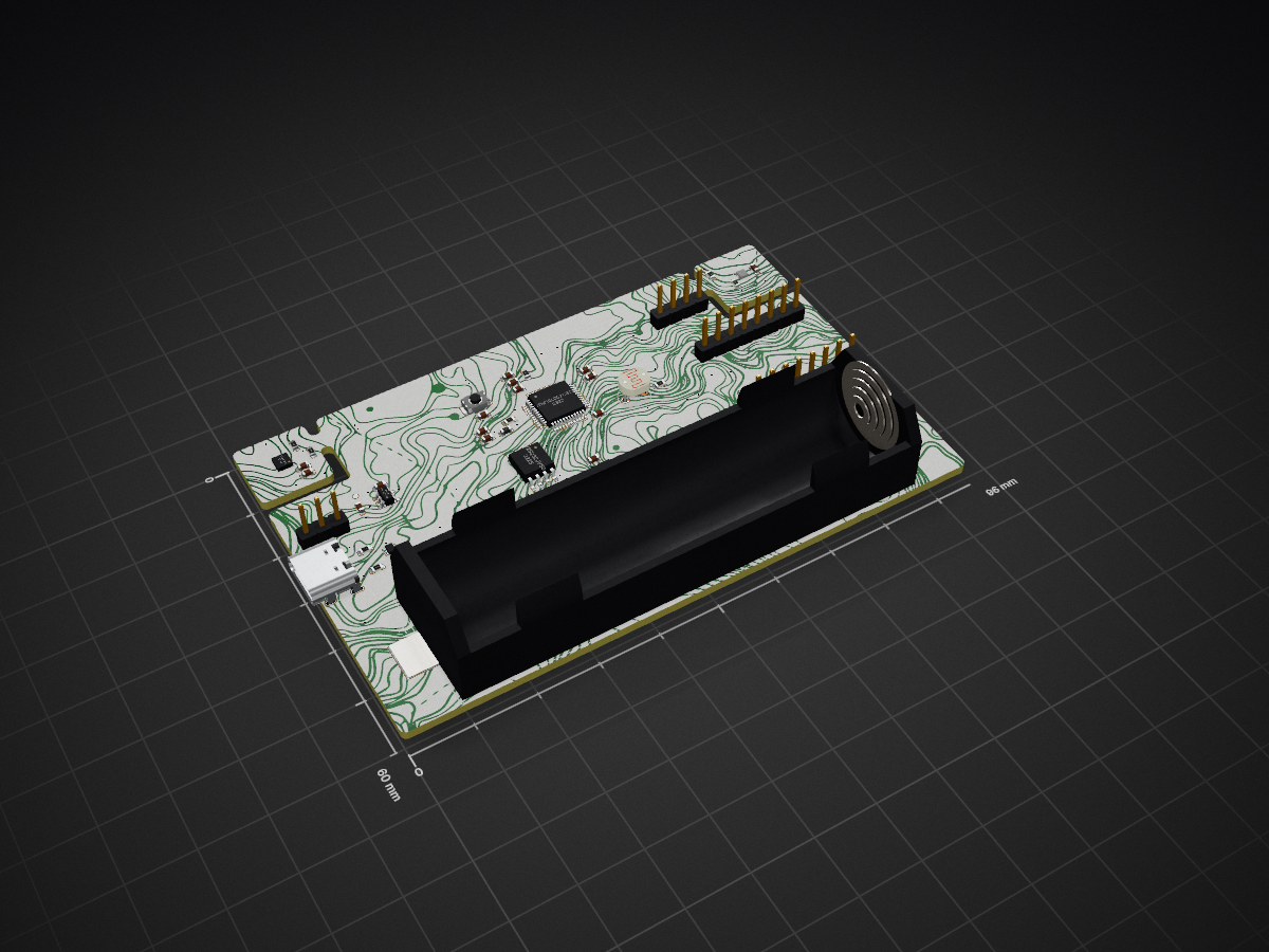
 souptik-samanta/Sensor-Node1
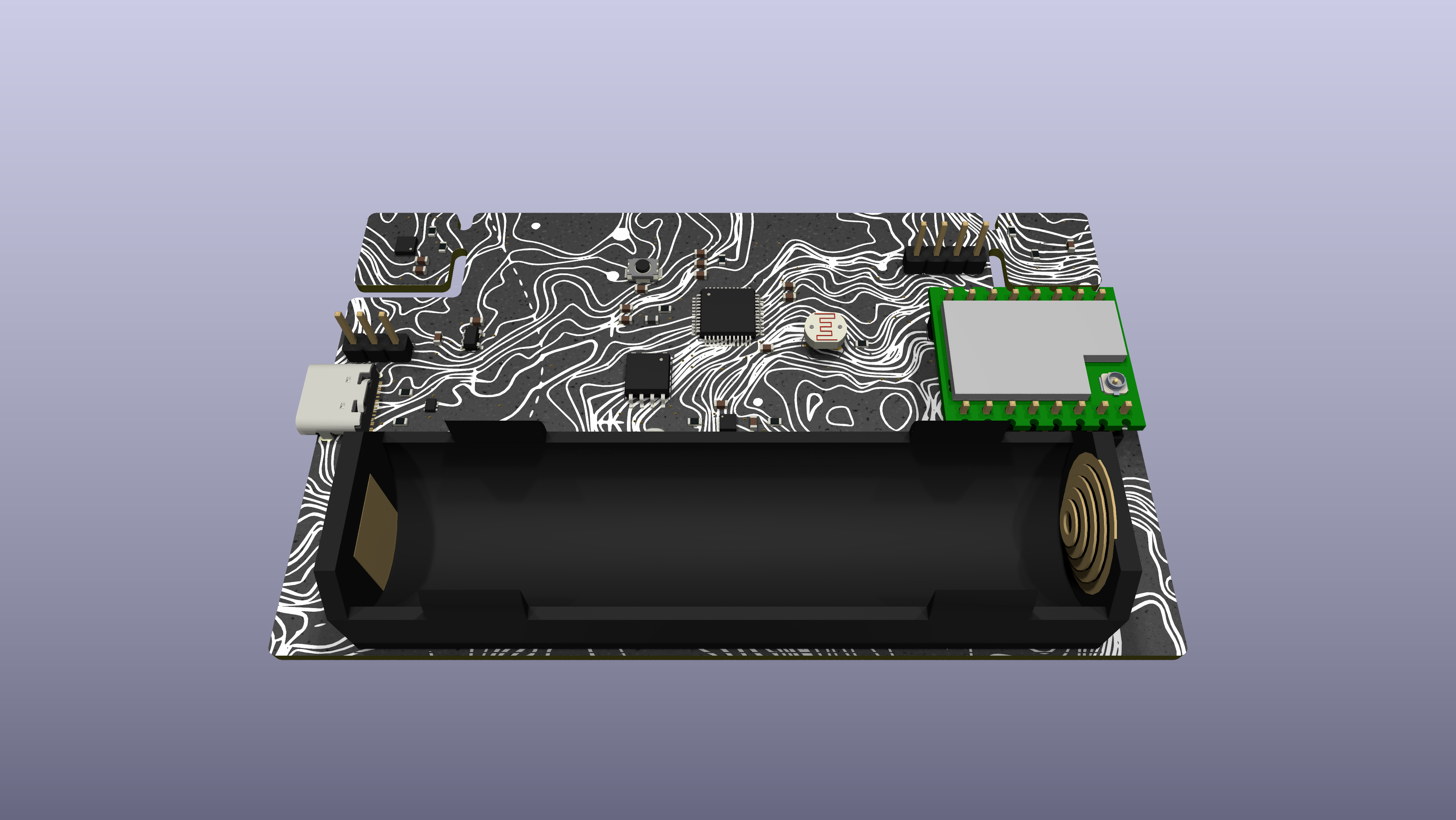
A compact environmental monitoring node built around the STM32L052 microcontroller. The board measures temperature, humidity, while providing onboard storage and support for external SX1262 LoRa modules.
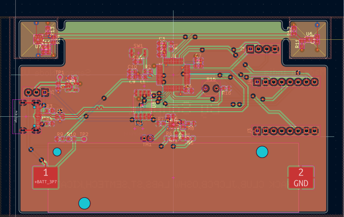
Sensor Node is an open-source printed circuit board by souptik-samanta, from the souptik-samanta/Sensor-Node repository on GitHub. It is a 4-layer board of 96 × 60 mm with 59 parts on 65 nets, routed with 384 tracks and 75 vias.
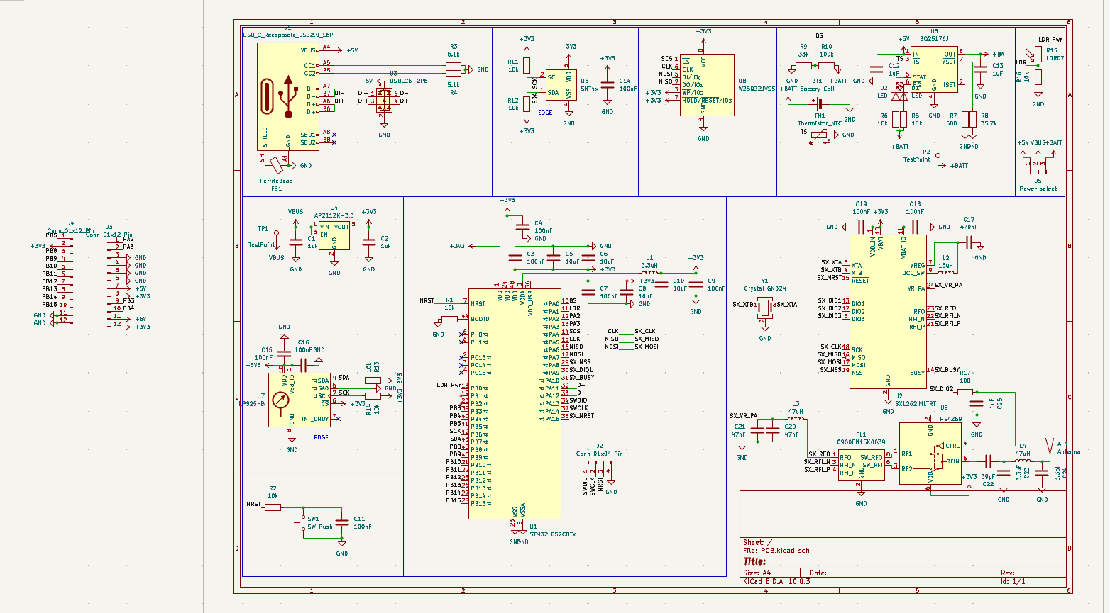
It is built around the LPS25HB, W25Q32JVSSIQ and AP2112K-3.3, with the BQ25176JDSG and USBLC6-2P6 among its other parts. Its parts include 16 capacitors, 16 resistors, 7 ICs, 5 connectors and 2 diodes. It belongs with the home automation and IoT and sensors and measurement boards and the STM32 boards of this library.


A compact environmental monitoring node built around the STM32L052 microcontroller. The board measures temperature, humidity, while providing onboard storage and support for external SX1262 LoRa modules.
I wanted to design a low-power sensor platform that could be deployed outdoors for long periods while collecting environmental data. Instead of using multiple development boards, I designed a custom PCB that integrates sensing, power management, storage, and expansion capabilities into a single board.
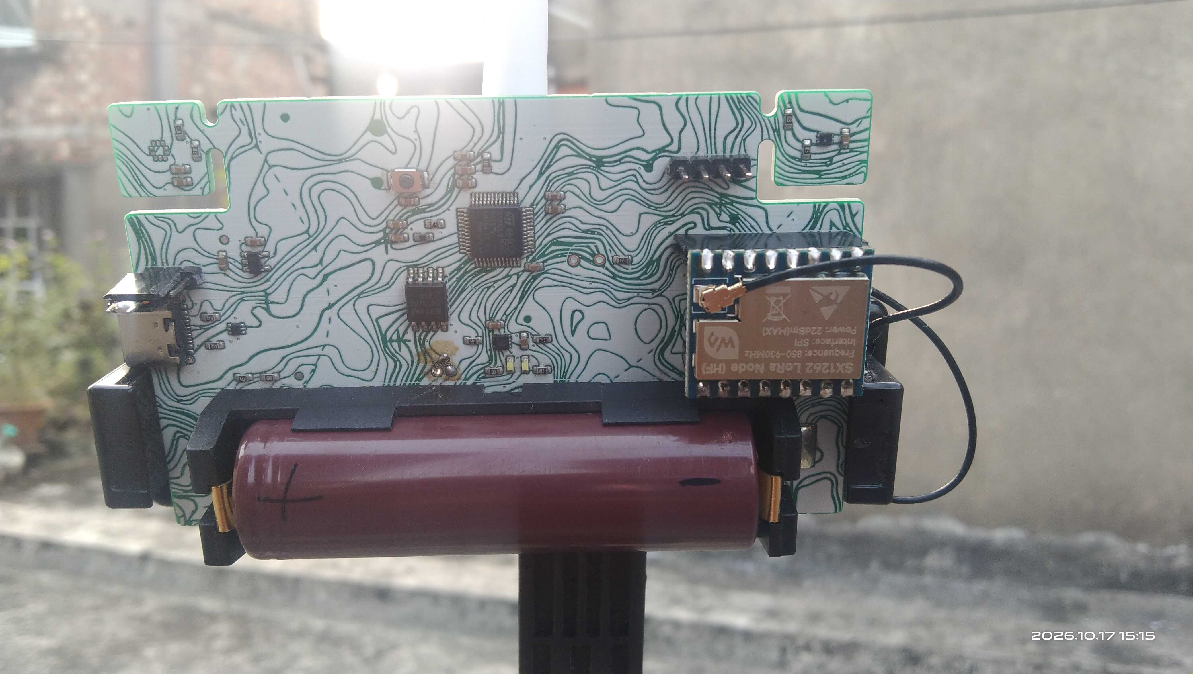
The firmware is responsible for:
| Designator | Quantity | Value / Part |
|---|---|---|
| BT1 | 1 | 18650 Battery Holder (Keystone 1042) |
| C1, C2, C12, C13 | 4 | 1µF Capacitor (0603) |
| C5, C6, C8, C10 | 4 | 4.7µF Capacitor (0603) |
| C3, C4, C7, C9, C11, C14, C15, C16 | 8 | 100nF Capacitor (0603) |
| D1, D2 | 2 | LED (0603) |
| J1 | 1 | USB-C Receptacle (USB4105-xx-A) |
| J2 | 1 | 1x4 Pin Header |
| J3, J4 | 2 | 1x8 Pin Header |
| J5 | 1 | Power Select Header |
| L1 | 1 | 3.3µH Inductor |
| R1, R2, R5, R6, R11, R12, R13, R14, R16 | 9 | 10kΩ Resistor (0603) |
| R10 | 1 | 100kΩ Resistor (0603) |
| R15 | 1 | LDR07 Light Dependent Resistor |
| R3, R4 | 2 | 5.1kΩ Resistor (0603) |
| R7 | 1 | 600Ω Resistor (0603) |
| R8 | 1 | 35.7kΩ Resistor (0603) |
| R9 | 1 | 33kΩ Resistor (0603) |
| SW1 | 1 | Push Button Switch (SKRK Series) |
| TH1 | 1 | NTC Thermistor |
| TP1, TP2, TP4, TP5, TP6 | 5 | Test Point |
| U1 | 1 | STM32L052C8Tx Microcontroller |
| U3 | 1 | USBLC6-2P6 USB ESD Protection |
| U4 | 1 | AP2112K-3.3 Voltage Regulator |
| U5 | 1 | BQ25176J Battery Charger |
| U6 | 1 | SHT4x Temperature & Humidity Sensor |
| U7 | 1 | LPS25HB Pressure Sensor |
| U8 | 1 | W25Q32JVSS SPI Flash Memory |
| Item | Cost |
|---|---|
| PCB + PCBA (JLCPCB) | $70 |
| Shipping | $24 |
| Total | $94 |
The firmware can be uploaded to the board through the SWD programming interface using an ST-LINK debugger.
SWDIO to SWDIOSWCLK to SWCLKGND to GND3V3 to the target voltage/reference pin, if required by the debuggerNRST as well when using reset-under-connectSensorNode Code folder.SensorNode project and click Build. The compiled firmware is generated at SensorNode Code/Debug/SensorNode.elf.To upload a later firmware change, build the project again and repeat step 6. The project is configured for SWD programming of the STM32L051C8Tx; the USB-C connector should only be used for programming if a compatible USB bootloader has been added to the firmware.
| Qty | Value | Footprint | References |
|---|---|---|---|
| 9 | 10k | Resistor_SMD:R_0603_1608Metric | R1, R2, R5, R6, R11, R12, R13, R14, R16 |
| 8 | 100nF | Capacitor_SMD:C_0603_1608Metric | C3, C4, C7, C9, C11, C14, C15, C16 |
| 5 | TestPoint | TestPoint:TestPoint_Pad_D1.0mm | TP1, TP2, TP4, TP5, TP6 |
| 4 | 1uF | Capacitor_SMD:C_0603_1608Metric | C1, C2, C12, C13 |
| 4 | 4.7uF | Capacitor_SMD:C_0603_1608Metric | C5, C6, C8, C10 |
| 4 | LOGO | LOGO | G***, G***, G***, G*** |
| 2 | 5.1k | Resistor_SMD:R_0603_1608Metric | R3, R4 |
| 2 | Conn_01x08_Pin | Connector_PinHeader_2.54mm:PinHeader_1x08_P2.54mm_Vertical | J3, J4 |
| 2 | LED | LED_SMD:LED_0603_1608Metric | D1, D2 |
| 1 | 100k | Resistor_SMD:R_0603_1608Metric | R10 |
| 1 | 3.3uH | Inductor_SMD:L_0603_1608Metric | L1 |
| 1 | 33k | Resistor_SMD:R_0603_1608Metric | R9 |
| 1 | 35.7k | Resistor_SMD:R_0603_1608Metric | R8 |
| 1 | 600 | Resistor_SMD:R_0603_1608Metric | R7 |
| 1 | AP2112K-3.3 | Package_TO_SOT_SMD:SOT-23-5 | U4 |
| 1 | BQ25176J | Package_SON:WSON-8-1EP_2x2mm_P0.5mm_EP0.9x1.6mm | U5 |
| 1 | Battery_Cell | Battery:BatteryHolder_Keystone_1042_1x18650 | BT1 |
| 1 | Conn_01x04_Pin | Connector_PinHeader_2.54mm:PinHeader_1x04_P2.54mm_Vertical | J2 |
| 1 | LDR07 | OptoDevice:R_LDR_5.1x4.3mm_P3.4mm_Vertical | R15 |
| 1 | LPS25HB | Package_LGA:ST_HLGA-10_2.5x2.5mm_P0.6mm_LayoutBorder3x2y | U7 |
| 1 | Power select | Connector_PinHeader_2.54mm:PinHeader_1x03_P2.54mm_Vertical | J5 |
| 1 | SHT4x | Sensor_Humidity:Sensirion_DFN-4_1.5x1.5mm_P0.8mm_SHT4x_NoCentralPad | U6 |
| 1 | STM32L052C8Tx | Package_QFP:LQFP-48_7x7mm_P0.5mm | U1 |
| 1 | SW_Push | Button_Switch_SMD:SW_Push_SPST_NO_Alps_SKRK | SW1 |
| 1 | Thermistor_NTC | Resistor_THT:R_Axial_DIN0204_L3.6mm_D1.6mm_P1.90mm_Vertical | TH1 |
| 1 | USBLC6-2P6 | Package_TO_SOT_SMD:SOT-666 | U3 |
| 1 | USB_C_Receptacle_USB2.0_16P | Connector_USB:USB_C_Receptacle_GCT_USB4105-xx-A_16P_TopMnt_Horizontal | J1 |
| 1 | W25Q32JVSS | Package_SO:SOIC-8_5.3x5.3mm_P1.27mm | U8 |
It measures 96 × 60 mm and has 4 copper layers, 1.6 mm thick.
59 parts, built around the LPS25HB, W25Q32JVSSIQ, AP2112K-3.3 and BQ25176JDSG. The full list of its parts is on this page, with links to each part's symbol and footprint where PCBKit's library has them.
From the souptik-samanta/Sensor-Node repository on GitHub, at the commit this page was made from: the board is PCB/PCB.kicad_pcb and its schematic PCB/PCB.kicad_sch. PCBKit opens the board in the browser, with nothing to install.
Its repository states no licence, so its author keeps all rights: ask souptik-samanta before reusing the design.

tynix5/no_fly_zone
STM32-based quadcopter and remote controller running on custom hardware and software


pdaslabs08/ESP32-and-IOT_Project1
Custom 4-layer ESP32 IoT PCB designed in KiCad with complete schematic, PCB layout, and manufacturing-ready files.


Shubhamai/tsar
General-purpose & fully programmable flight computer PCB desgined in KiCad EDA