4 layers38.5 × 19.5 mm

 sneakylizard123-4/ESP32-S3_Module
This is a small, self-contained development board built around the ESP32-S3-WROOM-1U. The idea is a go-to prototyping board: drop in a LiPo, plug in USB-C, and you have a programmable ESP32-S3 with WiFi/BLE/Zigbee, a…
ESP32-S3 Module is an open-source printed circuit board by sneakylizard123-4, from the sneakylizard123-4/ESP32-S3_Module repository on GitHub, published under the CERN-OHL-P-2.0 licence. It is a 4-layer board of 30 × 73 mm with 53 parts on 62 nets, routed with 490 tracks and 94 vias.
It is built around the ESP32-S3-WROOM-1-N8, IP5306 and TLV75733PDBV, with the USBLC6-2SC6 and WS2812B among its other parts. Its parts include 17 capacitors, 11 resistors, 8 diodes, 4 ICs and 4 connectors. It belongs with the radio and wireless boards and the ESP32 boards of this library.


A Feather-like ESP32-S3 dev board with USB-C, IP5306 battery charging, an onboard NeoPixel, and status LEDs.
This is a small, self-contained development board built around the ESP32-S3-WROOM-1U. The idea is a go-to prototyping board: drop in a LiPo, plug in USB-C, and you have a programmable ESP32-S3 with WiFi/BLE/Zigbee, a NeoPixel for quick visual feedback, and a full set of 2.54mm breakouts. I made it because my other ESP32 boards were either not ESP32-S3, had no USB, or needed an external FTDI adapter just to flash.
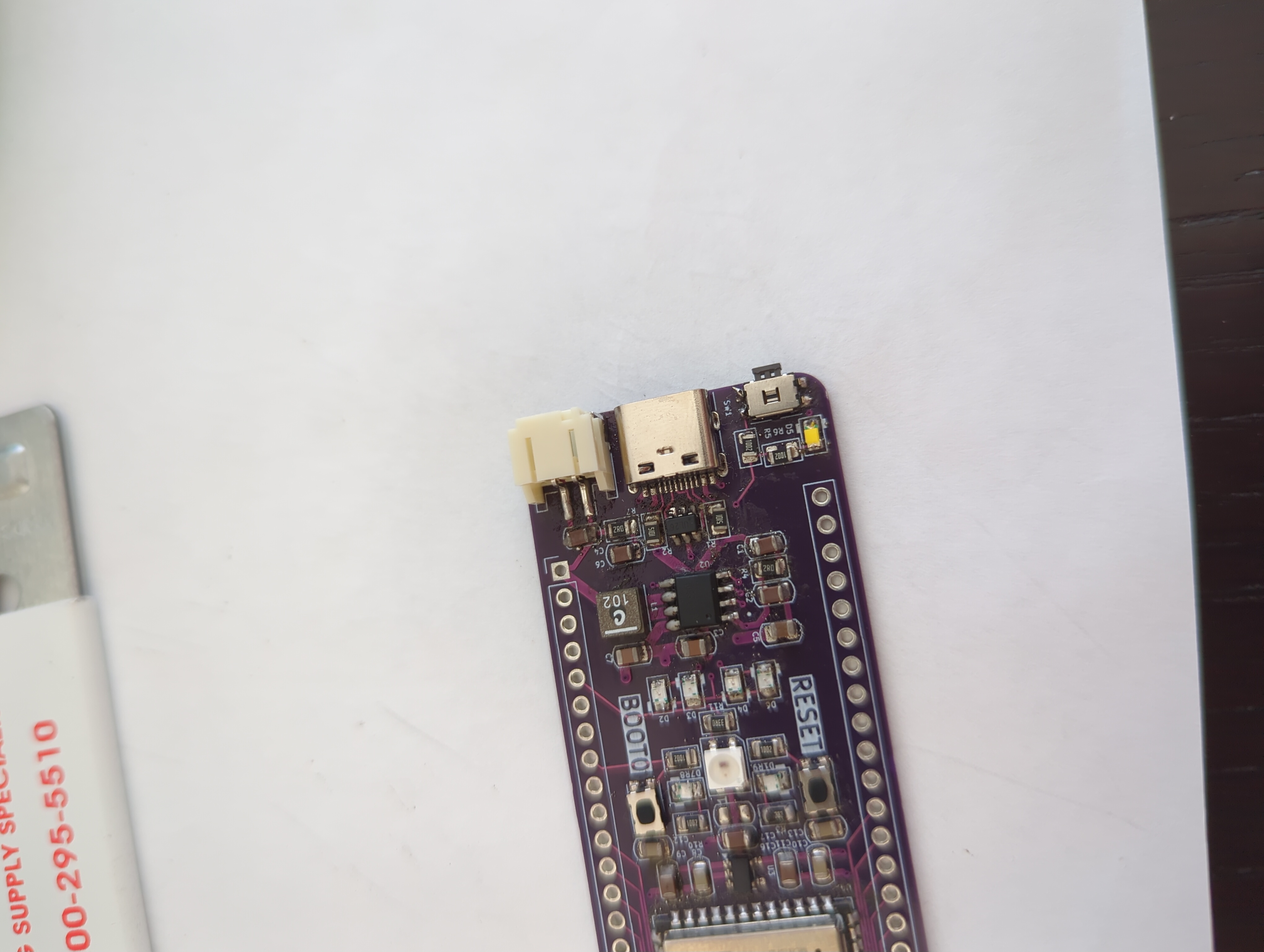
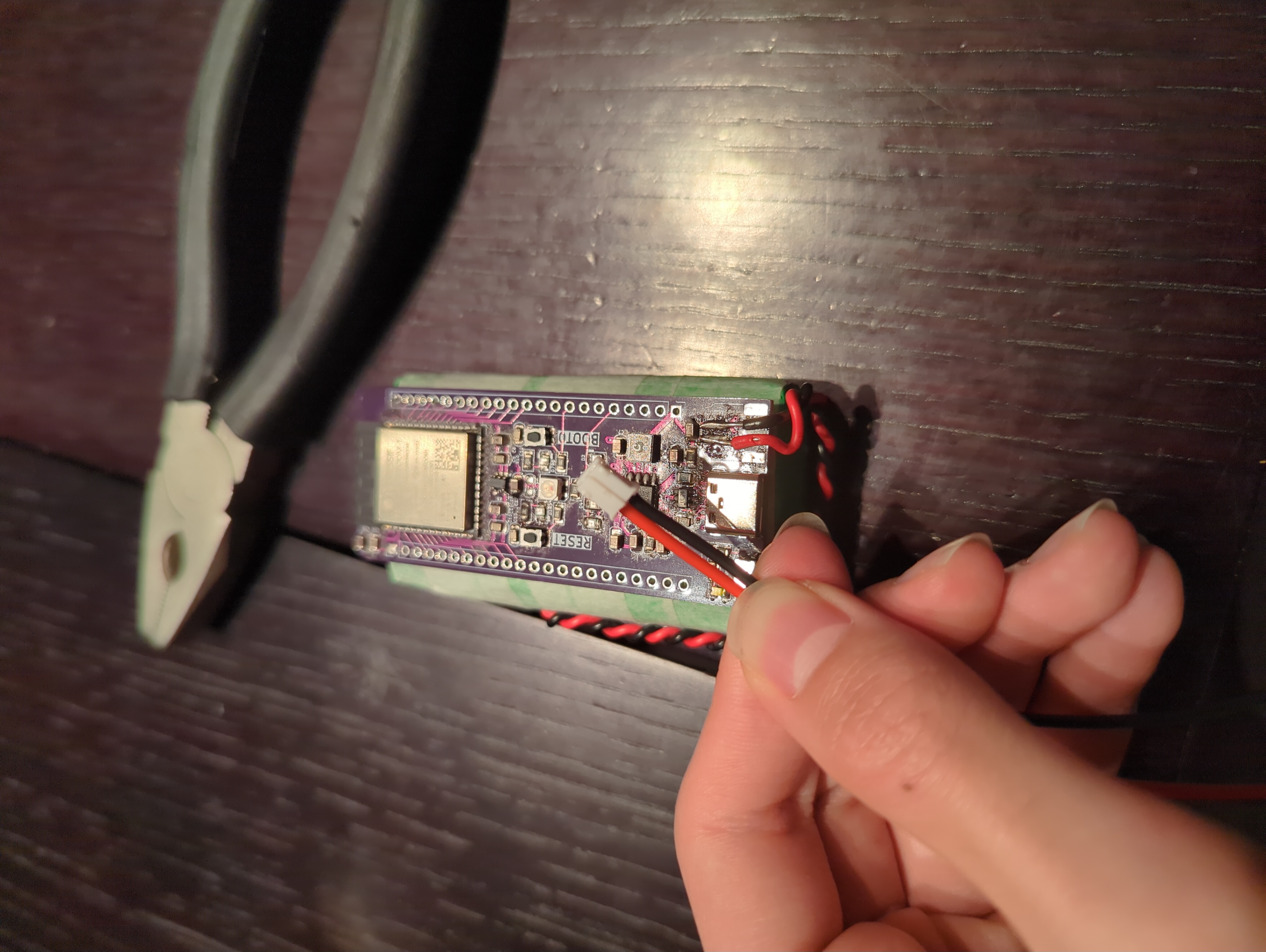
Build status: assembled and working. USB, charging, the NeoPixel, and the user LED have all been verified on the physical board. See proof/V1 for build photos and test results.
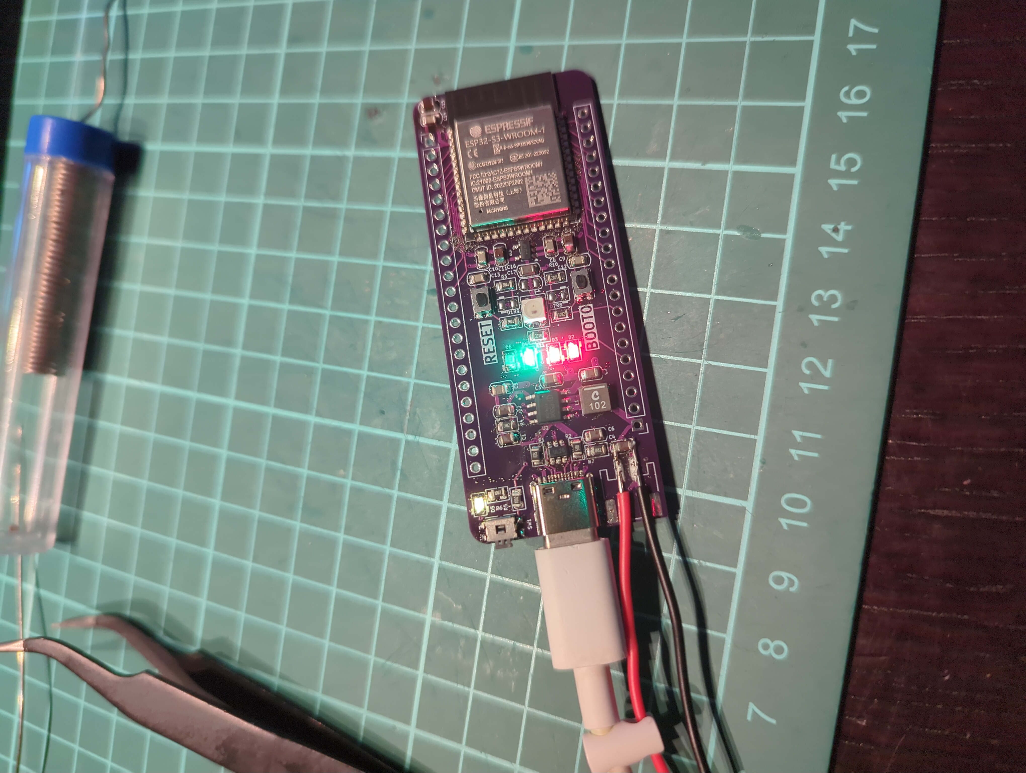
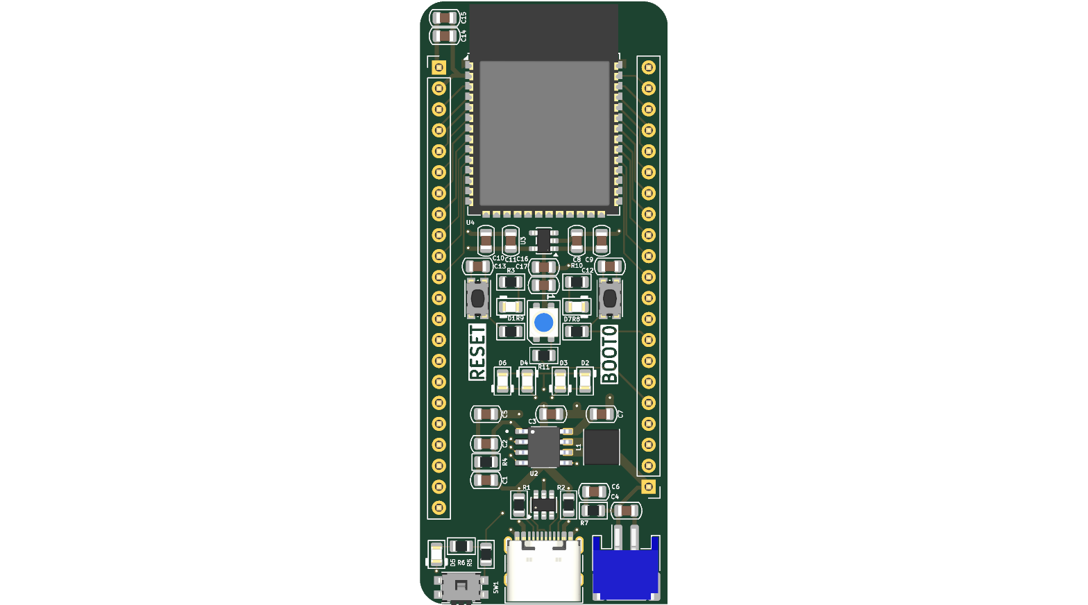
The board is four functional blocks plus a breakout. USB-C feeds the IP5306, which charges the LiPo and boosts it to a 5V rail. That rail powers the NeoPixel and feeds a TLV75733 LDO, which makes the 3.3V rail for the ESP32-S3. The MCU drives the NeoPixel on GPIO47 and the user LED on GPIO48, and breaks out its remaining IO on the two headers.
| Block | Key parts | What it does |
|---|---|---|
| USB input | J1, U1, R1, R2 | USB-C receptacle, ESD protection, and 5.1k CC resistors |
| Charging / boost | U2 (IP5306), L1, R7, C4, C6 | Charges the LiPo and boosts it to +5V, with a LED gauge |
| 3.3V supply | U3 (TLV75733), C3, C5, C7, C10 | LDO that turns +5V into +3.3V for the MCU and logic |
| MCU | U4 (ESP32-S3-WROOM-1U) | WiFi/BLE/Zigbee, native USB, U.FL antenna |
| Indicators | D1-D8, R6, R10, R11 | Power, charge gauge, power key, user LED, NeoPixel |
| Controls | SW1, SW2, SW3 | IP5306 power key, BOOT0, RESET |
| Breakout | J3, J4, J2 | 1x22 and 1x21 headers and a battery connector |
flowchart LR
  USB["USB-C VBUS"] --> IP5306["IP5306 (U2)"]
  BATT["LiPo JST-PH (J2)"] <--> IP5306
  IP5306 -->|+5V| NEO["WS2812B NeoPixel (D8)"]
  IP5306 -->|+5V| LDO["TLV75733 LDO (U3)"]
  LDO -->|+3.3V| ESP["ESP32-S3-WROOM-1U (U4)"]
  ESP -->|GPIO47| NEO
ESP -->|GPIO48| LED["User LED (D7)"]The board is a 4-layer PCB measuring 35.70 x 79.00 mm, with 1.6mm thickness and a dedicated ground inner layer. Power traces are widened and the edges are rounded for handling. Routing is done by hand in KiCad.
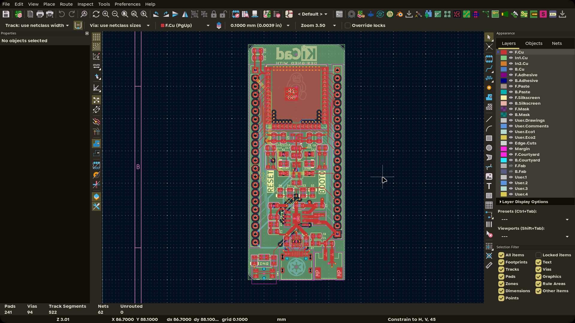
Schematic and PCB sources live in kicad/. Fabrication outputs (Gerbers, drill, BOM, pick-and-place) are in kicad/production/, and the STEP model is in cad/.
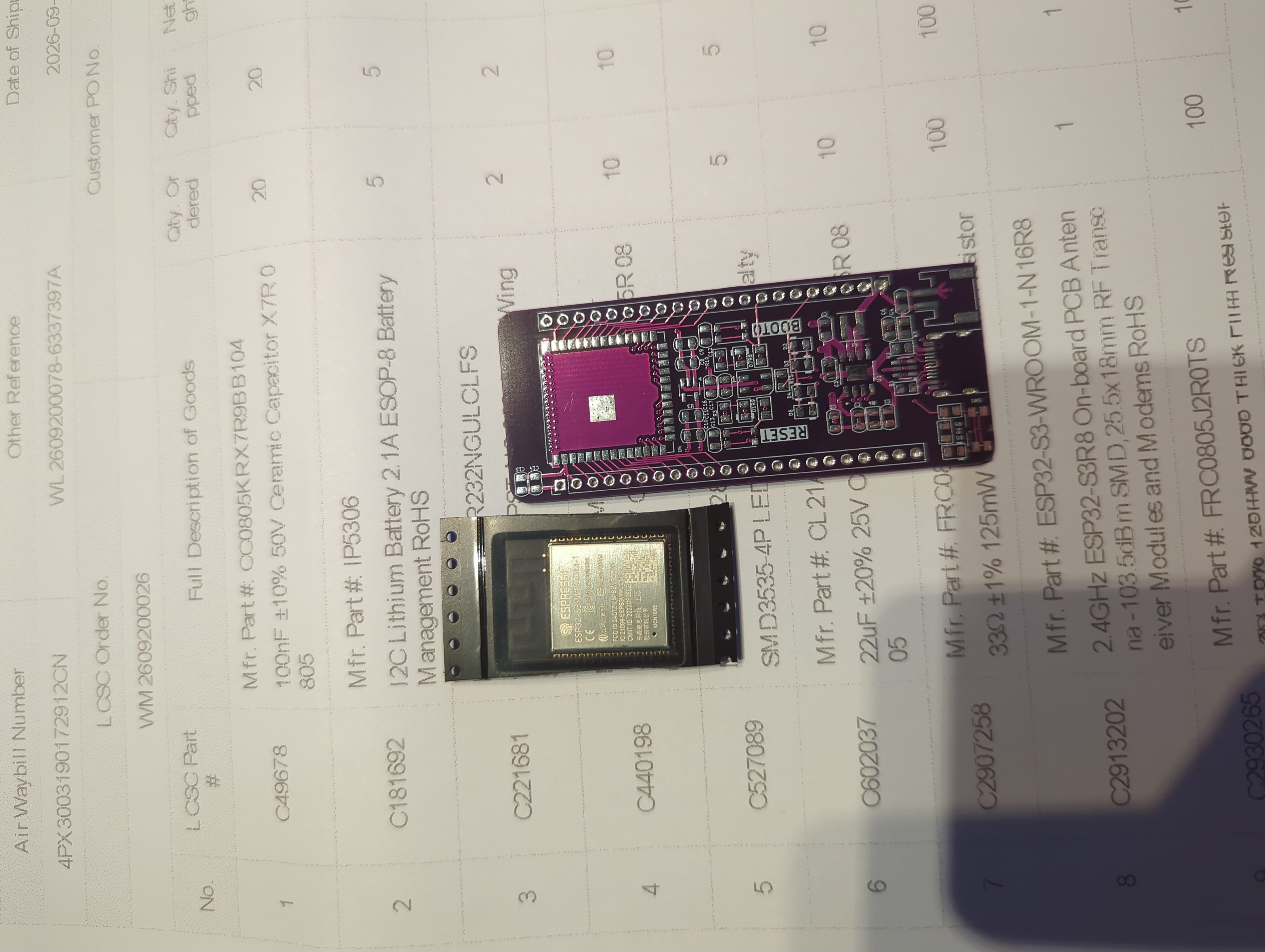
The board was assembled by hand: parts laid out and checked, the USB-C and power sections soldered first, then the headers and the JST-PH battery connector. After that came the power-on checks over USB-C and a power bank.
 |  |
 | 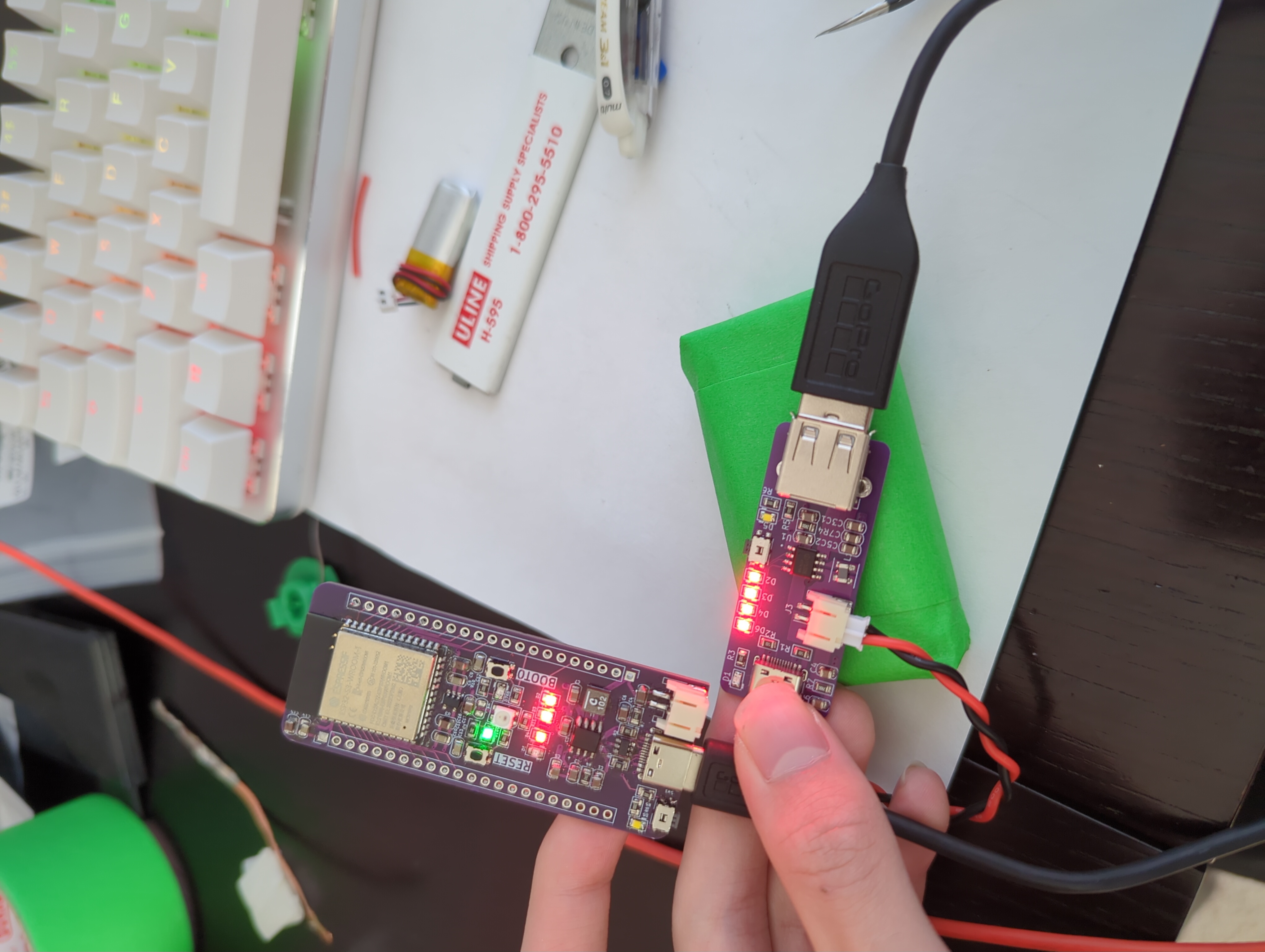 |
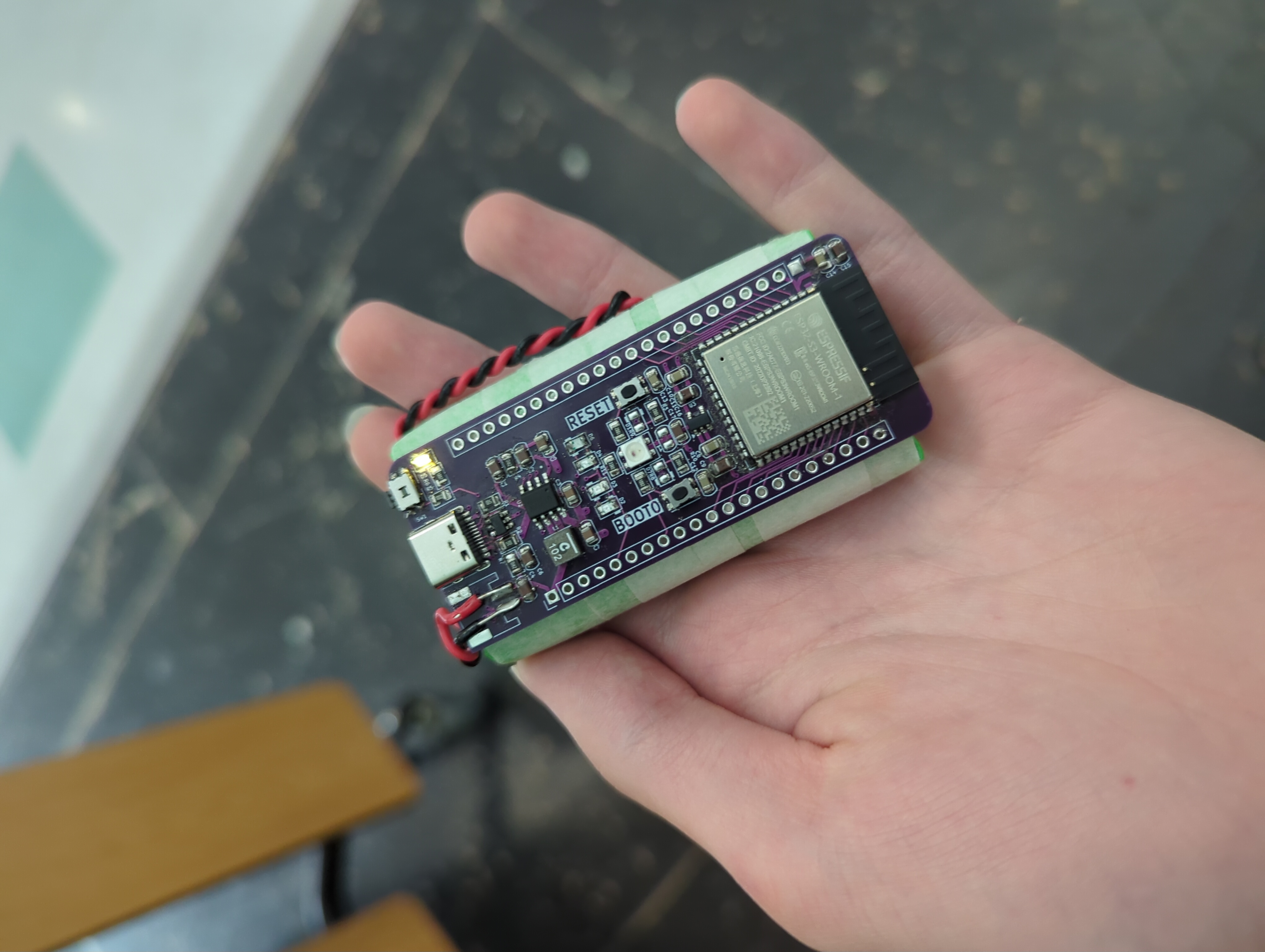
The NeoPixel and status LEDs running the self-test: video/neopixel.mp4.
More build and test detail: proof/V1/PROOF.md.
The firmware in firmware/ is an interactive self-test over USB CDC. It reports system info and power status, drives the NeoPixel and user LED, reads the BOOT button, runs a GPIO loopback check, and scans for WiFi and BLE networks. It is a PlatformIO project using the Arduino framework, the Adafruit NeoPixel library, and NimBLE-Arduino.
cd firmware
pio run                 # build
pio run --target upload # flash over USB
To enter the bootloader manually:
See firmware/README.md for the pin map and library details.
J3 - 1x22 header:
| Pin | Net | Pin | Net |
|---|---|---|---|
| 1 | GND | 12 | IO8 |
| 2 | +3.3V | 13 | USB_D- |
| 3 | EN | 14 | USB_D+ |
| 4 | IO4 | 15 | IO3 |
| 5 | IO5 | 16 | IO46 |
| 6 | IO6 | 17 | IO9 |
| 7 | IO7 | 18 | IO10 |
| 8 | IO15 | 19 | IO11 |
| 9 | IO16 | 20 | IO12 |
| 10 | IO17 | 21 | +5V |
| 11 | IO18 | 22 | VBUS |
J4 - 1x21 header:
| Pin | Net | Pin | Net |
|---|---|---|---|
| 1 | +BATT | 12 | IO38 |
| 2 | IO13 | 13 | IO39 |
| 3 | IO14 | 14 | IO40 |
| 4 | IO21 | 15 | IO41 |
| 5 | IO47 (NeoPixel) | 16 | IO42 |
| 6 | IO48 (User LED) | 17 | RXD0 |
| 7 | IO45 | 18 | TXD0 |
| 8 | IO0 (BOOT) | 19 | IO2 |
| 9 | IO35 | 20 | IO1 |
| 10 | IO36 | 21 | GND |
| 11 | IO37 |
Note: IO0, IO3, IO45, IO46 are ESP32-S3 strapping pins. Pull them the wrong way at boot and the chip enters a different mode.
| Ref | Value | Qty | Unit $ | Ext $ |
|---|---|---|---|---|
| C1, C2, C4, C6, C9, C11, C15, C17 | 10uF 25V X5R 0805 | 8 | 0.0871 | 0.6968 |
| C8, C10, C12, C13, C14, C16 | 100nF 50V X7R 0805 | 6 | 0.0266 | 0.1596 |
| C3, C5, C7 | 22uF 25V X5R 0805 | 3 | 0.0698 | 0.2094 |
| D1-D7 | Orange LED 0805 | 7 | 0.0096 | 0.0672 |
| D8 | WS2812B NeoPixel | 1 | 0.0940 | 0.0940 |
| J1 | USB-C receptacle 16P | 1 | 0.1724 | 0.1724 |
| J2 | JST-PH 2P 2mm | 1 | 0.0356 | 0.0356 |
| J3 | Pin header 1x22 2.54mm | 1 | 0.1200 | 0.1200 |
| J4 | Pin header 1x21 2.54mm | 1 | 0.1000 | 0.1000 |
| L1 | 1uH shielded inductor | 1 | 2.5134 | 2.5134 |
| R1, R2 | 5.1k 1% 0805 | 2 | 0.0065 | 0.0130 |
| R3, R5, R6, R8, R9, R10 | 10k 1% 0805 | 6 | 0.0035 | 0.0210 |
| R11 | 330 1% 0805 | 1 | 0.0050 | 0.0050 |
| R4, R7 | 2R 1% 0805 | 2 | 0.0261 | 0.0522 |
| SW1 | Tactile switch EVQPUD | 1 | 0.2299 | 0.2299 |
| SW2, SW3 | Tactile switch KMR2 | 2 | 0.6515 | 1.3030 |
| U1 | USBLC6-2SC6 | 1 | 0.0896 | 0.0896 |
| U2 | IP5306 | 1 | 0.2989 | 0.2989 |
| U3 | TLV75733PDBV | 1 | 0.1819 | 0.1819 |
| U4 | ESP32-S3-WROOM-1U (N8) | 1 | 3.1300 | 3.1300 |
| PCB | Bare PCB (4-layer) | 1 | 1.5000 | 1.5000 |
| Total | 49 | 10.9929 |
Full BOM with LCSC part numbers, manufacturers, and supplier links: BOM.csv. KiCad-generated BOM and pick-and-place: kicad/production/bom.csv, kicad/production/positions.csv.
The board is designed for JLCPCB's standard 4-layer process:
.
|-- BOM.csv                 # Full bill of materials with supplier links
|-- README.md
|-- JOURNAL.md              # Build journal
|-- TIMELINE.md
|-- TODO.md                 # Ideas for v2
|-- cad/                    # STEP model
|-- firmware/               # PlatformIO firmware (Arduino)
|-- images/                 # Schematic, PCB, and render images
|-- kicad/                  # KiCad sources and production outputs
|-- proof/                  # Build and test proof
|-- LICENSE                 # CERN-OHL-P-2.0 (hardware)
`-- LICENSE-MIT # MIT (firmware)CERN-OHL-P-2.0. See LICENSE.firmware/): MIT License. SPDX: MIT. See LICENSE-MIT.| Qty | Value | Footprint | References |
|---|---|---|---|
| 8 | 10uF | Capacitor_SMD_AKL:C_0805_2012Metric | C1, C2, C4, C6, C9, C11, C15, C17 |
| 7 | LED | LED_SMD_AKL:LED_0805_2012Metric | D1, D2, D3, D4, D5, D6, D7 |
| 6 | 100nF | Capacitor_SMD_AKL:C_0805_2012Metric | C8, C10, C12, C13, C14, C16 |
| 6 | 10k | Resistor_SMD_AKL:R_0805_2012Metric | R3, R5, R6, R8, R9, R10 |
| 3 | 22uF | Capacitor_SMD_AKL:C_0805_2012Metric | C3, C5, C7 |
| 2 | 2 | Resistor_SMD_AKL:R_0805_2012Metric | R4, R7 |
| 2 | 5.1k | Resistor_SMD_AKL:R_0805_2012Metric | R1, R2 |
| 2 | SW_Push | Button_Switch_SMD:SW_Push_1P1T_NO_CK_KMR2 | SW2, SW3 |
| 1 | 1uH XFL4020-102MEC | Inductor_SMD:L_Coilcraft_XxL4020 | L1 |
| 1 | 330 | Resistor_SMD_AKL:R_0805_2012Metric | R11 |
| 1 | Conn_01x02 | Connector_JST_SM4:JST_PH_S2B-PH-SM4-TB_1x02-1MP_P2.00mm_Horizontal | J2 |
| 1 | Conn_01x21 | Connector_PinHeader_2.54mm:PinHeader_1x21_P2.54mm_Vertical | J4 |
| 1 | Conn_01x22 | Connector_PinHeader_2.54mm:PinHeader_1x22_P2.54mm_Vertical | J3 |
| 1 | ESP32-S3-WROOM-1 | RF_Module:ESP32-S3-WROOM-1U | U4 |
| 1 | IP5306 | IP5306:SOP127P600X165-9N | U2 |
| 1 | LOGO | customimages:linuxpenguin_cu | G*** |
| 1 | LOGO | customimages:empire_cu | G*** |
| 1 | LOGO | customimages:empire_mask | G*** |
| 1 | LOGO | customimages:linuxpenguin-mask | G*** |
| 1 | SW_Push | Button_Switch_SMD:Panasonic_EVQPUM_EVQPUD | SW1 |
| 1 | TLV75733PDBV | Package_TO_SOT_SMD:SOT-23-5 | U3 |
| 1 | USBLC6-2SC6 | Package_TO_SOT_SMD:SOT-23-6 | U1 |
| 1 | USB_C_Receptacle_USB2.0_16P | Connector_USB:USB_C_Receptacle_HRO_TYPE-C-31-M-12 | J1 |
| 1 | WS2812B | LED_SMD:LED_WS2812B-Mini_PLCC4_3.5x3.5mm | D8 |
The 52 most common of 53 parts.

broedschroed/NeoChristmasTreeV2
ESP32-powered Christmas tree ornament: 66x WS2812 LEDs on a 4-wing dual-PCB tree, IR remote with learnable sleep timer, browser-based pattern editor, LDR auto-brightness

jeremy341/esp32-alarm-clock
ESP32 based radio-controlled alarm clock with TFT display and custom UI using a Customade software

jjhcwoo/Acculux-device
The objective of this project is to add functionality to the existing NIR Imaging Inc. device in the way of: - Orientation tracking - Positional tracking - Force sensing

Snathan03-max/SWAMINATHAN_VIVEKANAND_2026A3PS1043H_JANUS_FINAL_SUBMISSION
Submission for JANUS round 3 Hackathon


petnica-rac-seminari/BCD-0o27-Tetris
The BalcCon Cyberdeck 0o27 (BCD-0o27) comes with a development framework that makes it easier to add functionality to the cyberdeck.
It measures 30 × 73 mm and has 4 copper layers, 1.6 mm thick.
53 parts, built around the ESP32-S3-WROOM-1-N8, IP5306, TLV75733PDBV and USBLC6-2SC6. The full list of its parts is on this page, with links to each part's symbol and footprint where PCBKit's library has them.
From the sneakylizard123-4/ESP32-S3_Module repository on GitHub, at the commit this page was made from: the board is kicad/ESP32-S3_Module.kicad_pcb and its schematic kicad/ESP32-S3_Module.kicad_sch. PCBKit opens the board in the browser, with nothing to install.
Its repository publishes it under the CERN-OHL-P-2.0 licence: you may reuse it on that licence's terms (keep the author's notice, and for a copyleft licence share your changes alike).