4 layers90.5 × 67 mm
AS 4
beaked99/air-scales
2025-11-20. Updated all the footprints and symbols to their proper layouts. no more fkn errors. Hallefuckinglujah. Fucked up with LM74610 not using the right footprint. minor fix. 2025-11-16.
131 parts

 smarthomefans/z2m_partner186
Hardware module for iobroker.zigbee
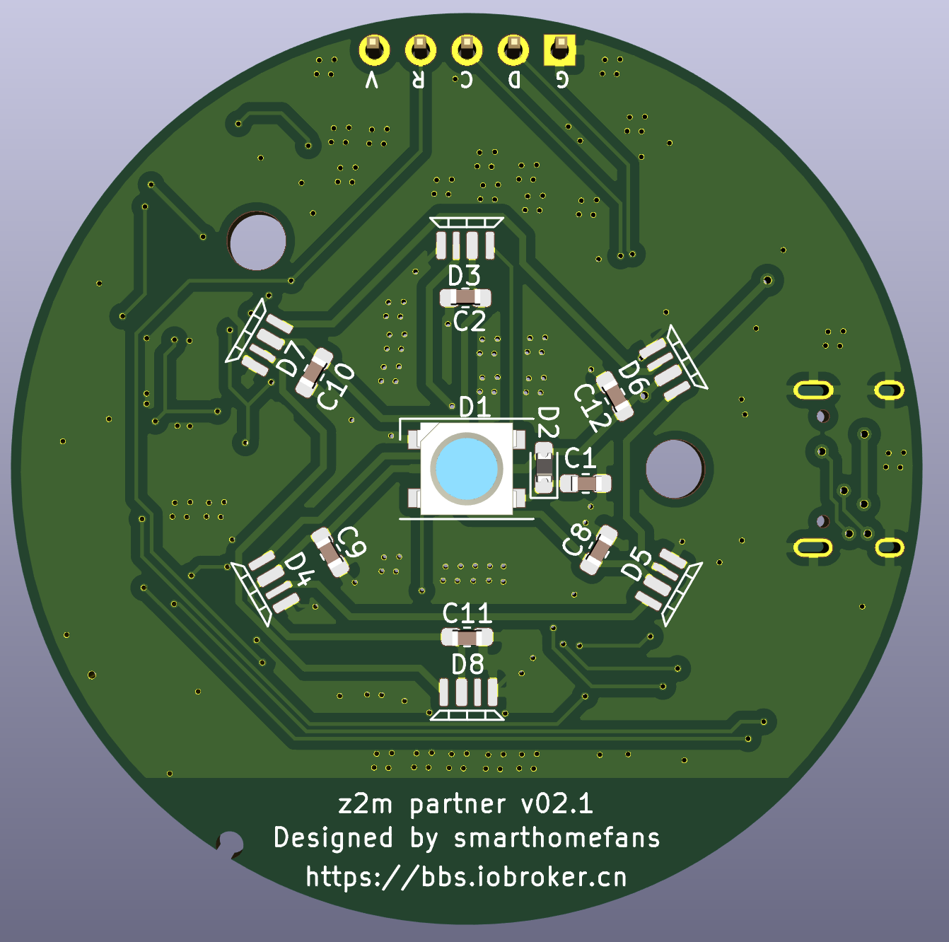
Z2m partner is an open-source printed circuit board by smarthomefans, from the smarthomefans/z2m_partner repository on GitHub. It is a 2-layer board of 13.7 × 21.4 mm with 52 parts on 66 nets, routed with 741 tracks and 224 vias.
It is built around the CH340C, E18-MS1PA1-IPX and ESP-WROOM-02, with the 74LVC1G66GW, AMS1117-3.3V and CD4052BM among its other parts. Its parts include 14 resistors, 12 capacitors, 8 diodes, 7 ICs and 3 switches. It belongs with the radio and wireless boards of this library.


This is hardware module for iobroker.zigbee and zigbee2mqtt or Zigbee to Tasmota.
If you can speak Chinese and be interested with this project, please look at this post in ioBroker China BBS
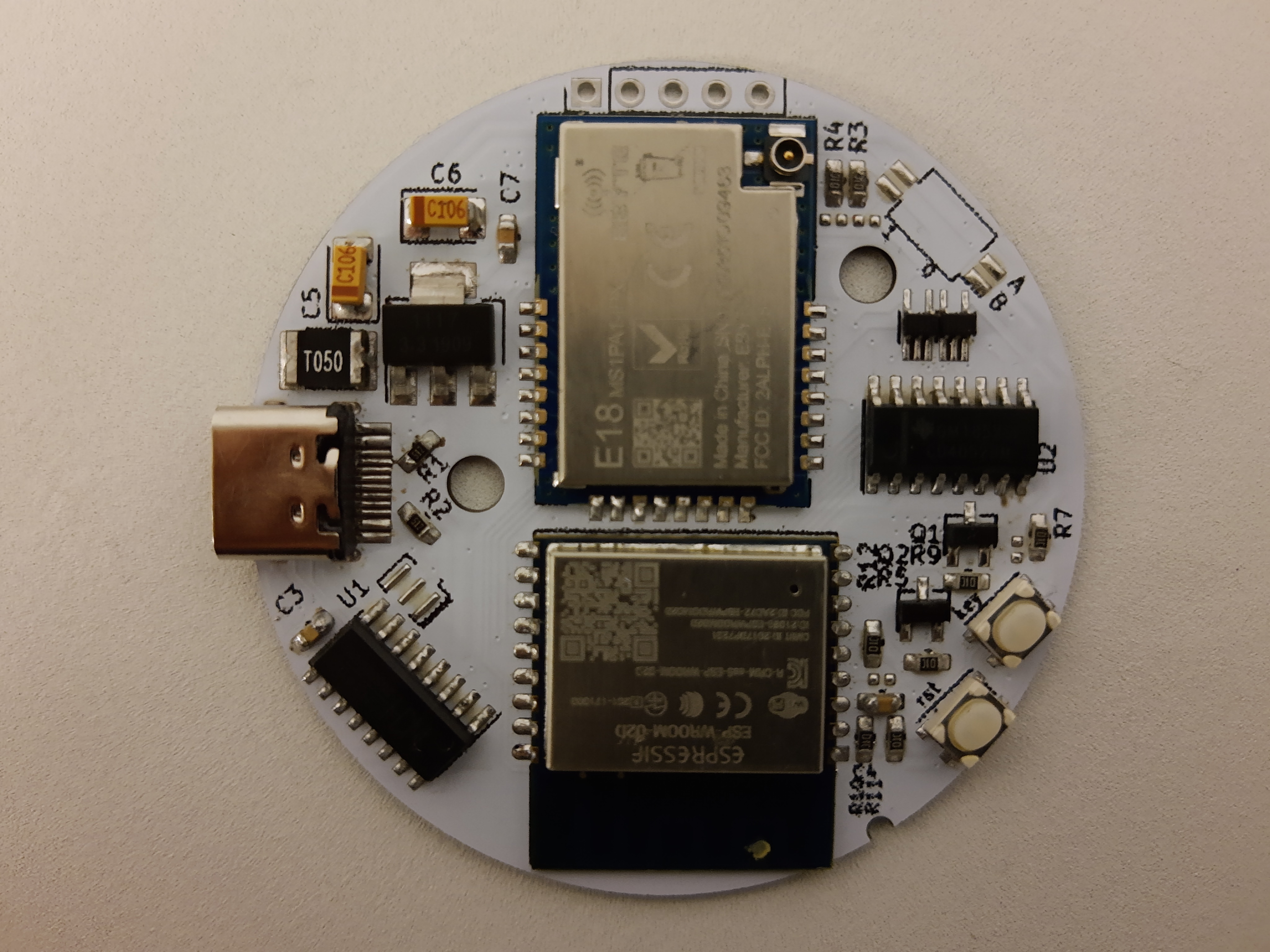
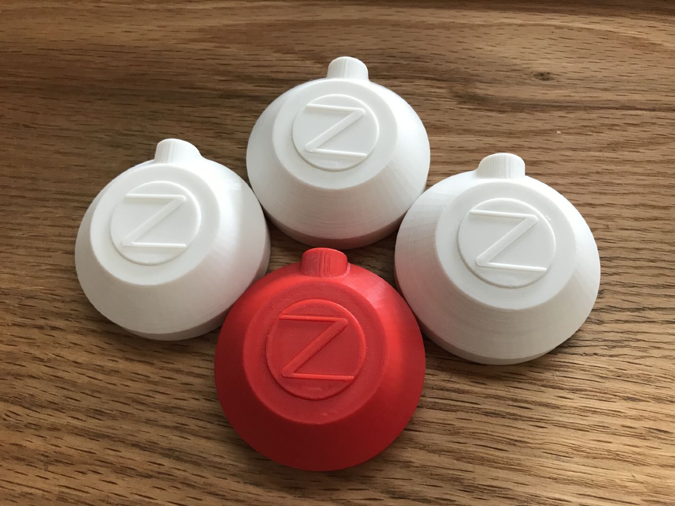
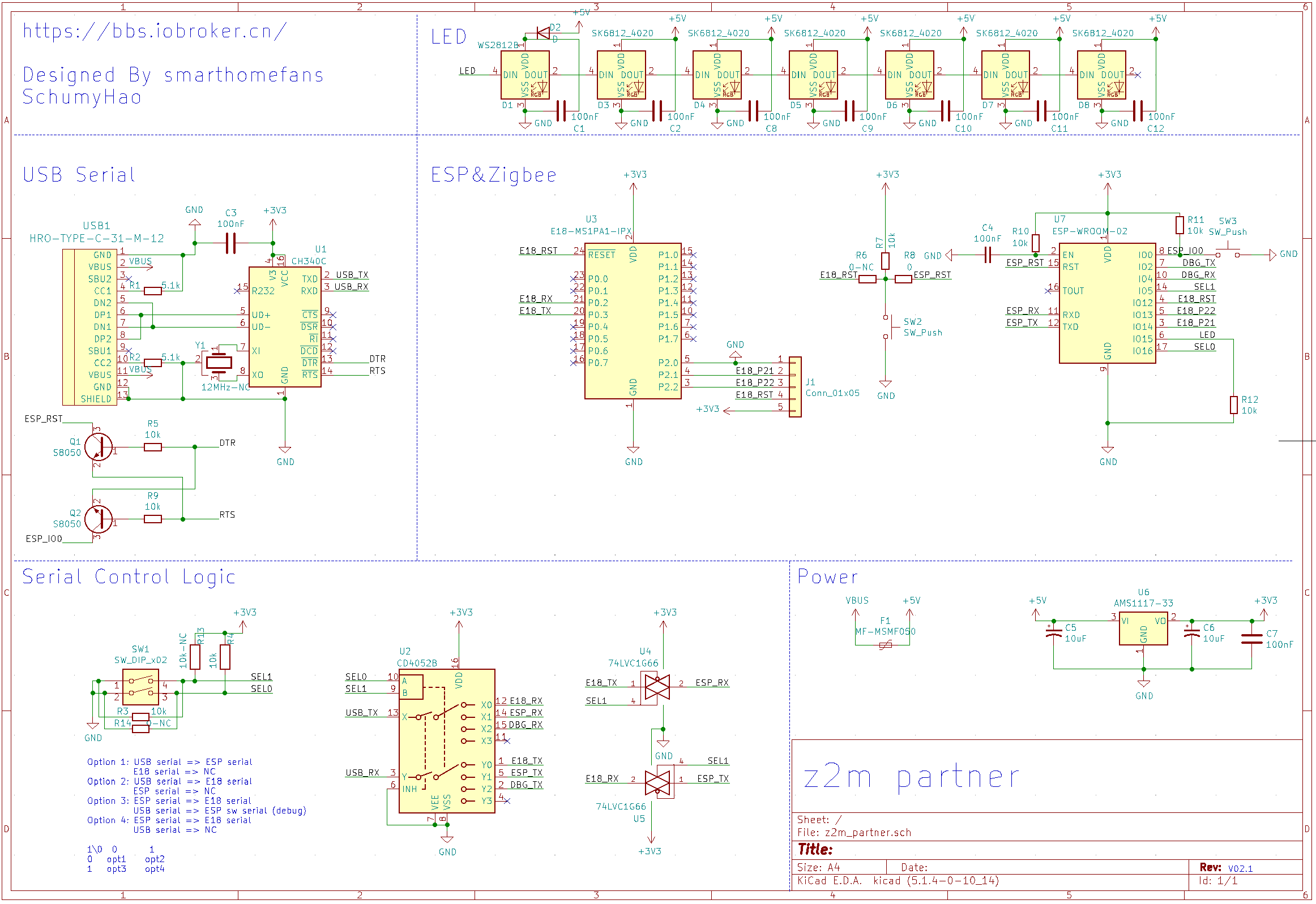
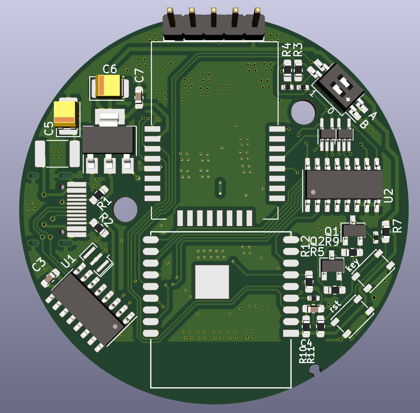
BOM can get from here.
| Qty | Value | Footprint | References |
|---|---|---|---|
| 10 | 100nF | Capacitor_SMD:C_0603_1608Metric_Pad1.05x0.95mm_HandSolder | C1, C2, C3, C4, C7, C8, C9, C10, C11, C12 |
| 8 | 10k | Resistor_SMD:R_0603_1608Metric_Pad1.05x0.95mm_HandSolder | R3, R4, R5, R7, R9, R10, R11, R12 |
| 6 | SK6812_4020 | z2m_partner:SK6812_4020 | D3, D4, D5, D6, D7, D8 |
| 2 | 0-NC | Resistor_SMD:R_0402_1005Metric | R6, R14 |
| 2 | 10uF | Capacitor_Tantalum_SMD:CP_EIA-3528-21_Kemet-B_Pad1.50x2.35mm_HandSolder | C5, C6 |
| 2 | 5.1k | Resistor_SMD:R_0603_1608Metric_Pad1.05x0.95mm_HandSolder | R1, R2 |
| 2 | 74LVC1G66 | Package_TO_SOT_SMD:SOT-353_SC-70-5_Handsoldering | U4, U5 |
| 2 | S8050 | Package_TO_SOT_SMD:TSOT-23 | Q1, Q2 |
| 2 | SW_Push | Button_Switch_SMD:SW_SPST_PTS810 | SW2, SW3 |
| 1 | 0 | Resistor_SMD:R_0402_1005Metric | R8 |
| 1 | 10k-NC | Resistor_SMD:R_0402_1005Metric | R13 |
| 1 | 12MHz-NC | Crystal:Resonator_SMD_muRata_CSTxExxV-3Pin_3.0x1.1mm | Y1 |
| 1 | AMS1117-33 | Package_TO_SOT_SMD:SOT-223-3_TabPin2 | U6 |
| 1 | CD4052B | Package_SO:SOIC-16_3.9x9.9mm_P1.27mm | U2 |
| 1 | CH340C | Package_SO:SOIC-16_3.9x9.9mm_P1.27mm | U1 |
| 1 | Conn_01x05 | Connector_PinHeader_2.54mm:PinHeader_1x05_P2.54mm_Vertical | J1 |
| 1 | D | Diode_SMD:D_0603_1608Metric_Pad1.05x0.95mm_HandSolder | D2 |
| 1 | E18-MS1PA1-IPX | z2m_partner:E18-MS1PA1-IPX | U3 |
| 1 | ESP-WROOM-02 | ESP8266:ESP-13-WROOM-02 | U7 |
| 1 | HRO-TYPE-C-31-M-12 | TypeC:HRO-TYPE-C-31-M-12-HandSoldering | USB1 |
| 1 | MF-MSMF050 | Fuse:Fuse_1812_4532Metric_Pad1.30x3.40mm_HandSolder | F1 |
| 1 | SW_DIP_x02 | Button_Switch_SMD:SW_DIP_SPSTx02_Slide_Copal_CHS-02B_W7.62mm_P1.27mm | SW1 |
| 1 | WS2812B | LED_SMD:LED_WS2812B_PLCC4_5.0x5.0mm_P3.2mm | D1 |
The 50 most common of 52 parts.
beaked99/air-scales
2025-11-20. Updated all the footprints and symbols to their proper layouts. no more fkn errors. Hallefuckinglujah. Fucked up with LM74610 not using the right footprint. minor fix. 2025-11-16.


denjhang/MegaGRRL-Desktop-Mini-USB
I have been using the desktop version of MegaGRRL for 4 years. As my PCB drawing skills improve, I have the confidence to realize all my ideas and changes.

Hanqaqa/Easyduino
Easily dive into different PCB KiCad designs of the most popular microcontroller devboards

SamyIOoOI/RetroCom
A 4-Station one-to-one two-way INTERCOM built around the AT89C52-PI24 RetroMCU (8051 Core).


It measures 13.7 × 21.4 mm and has 2 copper layers, 1.2 mm thick.
52 parts, built around the CH340C, E18-MS1PA1-IPX, ESP-WROOM-02 and 74LVC1G66GW. The full list of its parts is on this page, with links to each part's symbol and footprint where PCBKit's library has them.
From the smarthomefans/z2m_partner repository on GitHub, at the commit this page was made from: the board is project/z2m_partner.kicad_pcb. PCBKit opens the board in the browser, with nothing to install.
Its repository states no licence, so its author keeps all rights: ask smarthomefans before reusing the design.