4 layers253.6 × 137.7 mm
S100 Thunder186-1.0-006
RichCini/LomasBoards
Small repository of files/data related to Lomas Data Products S-100 boards.
118 parts1

 sladek/SBC_8080_ECB
This is my attempt to build a single-board microcomputer based on the Intel 8080 CPU. It contains the following features:
8080 Board is an open-source printed circuit board by sladek, from the sladek/SBC_8080_ECB repository on GitHub. It is a 2-layer board of 160.5 × 100.2 mm with 112 parts on 290 nets, routed with 3,526 tracks and 488 vias.
It is built around the 74LS245SC, 74LS125DC and 74LS240DC, with the MAX232N, TC7660HEOA and 74LS32SC among its other parts. Its parts include 45 capacitors, 30 ICs, 11 resistors, 6 diodes and 4 connectors.


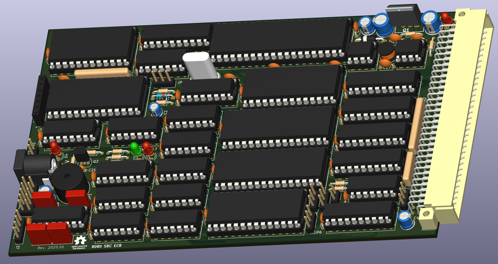
This is my attempt to build a single-board microcomputer based on the Intel 8080 CPU. It contains the following features:
Extended 512k x 8-bit SRAM that can be fully accessed via paging.
128 x 8-bit FLASH EPROM that is accessible after RESET so it can contain a bootloader, which can be moved to SRAM and boot the operating system or monitor program.
Programmable Interrupt Controller Intel 8259.
Programmable Interval Timer Intel 8253, which is used for baud rate generation and can also generate an interrupt and be connected to the speaker.
Universal Synchronous/Asynchronous Receiver/Transmitter (USART) Intel 8251 used as serial console so SBC can be accessed directly via RS232 interface.
ECB bus interface, which can be used for microcomputer extensions. The ECB bus interface facilitates communication between the main processor and various peripheral devices, enabling system expansion and enhancing functionality. Additionally, it allows for the integration of specialized hardware components, which can further optimize performance and adaptability in various applications. History of ECB bus is described below.
Voltage power supply for CPU: +5V, -5V, +12V which follows the requirement that -5V must be the first voltage present. It also contains inverter for -5V generation and a boost converter from 5V to 12V so the SBC can be powered only from one +5V power supply.
Here you can find a schematics for the SBC. Kicad files are also available in this repository. SBC_8080_ECB schematics.
(https://www.retrobrewcomputers.org/doku.php?id=boards:ecb:start)
Below is an image depicting the latest definition of the ECB bus as utilized by the RetroBrew Computers group. It also addresses issues related to the /RESET and /RESOUT pin definitions and the solutions implemented. This design incorporates a 3-pin jumper header to allow for the selection of the appropriate configuration.
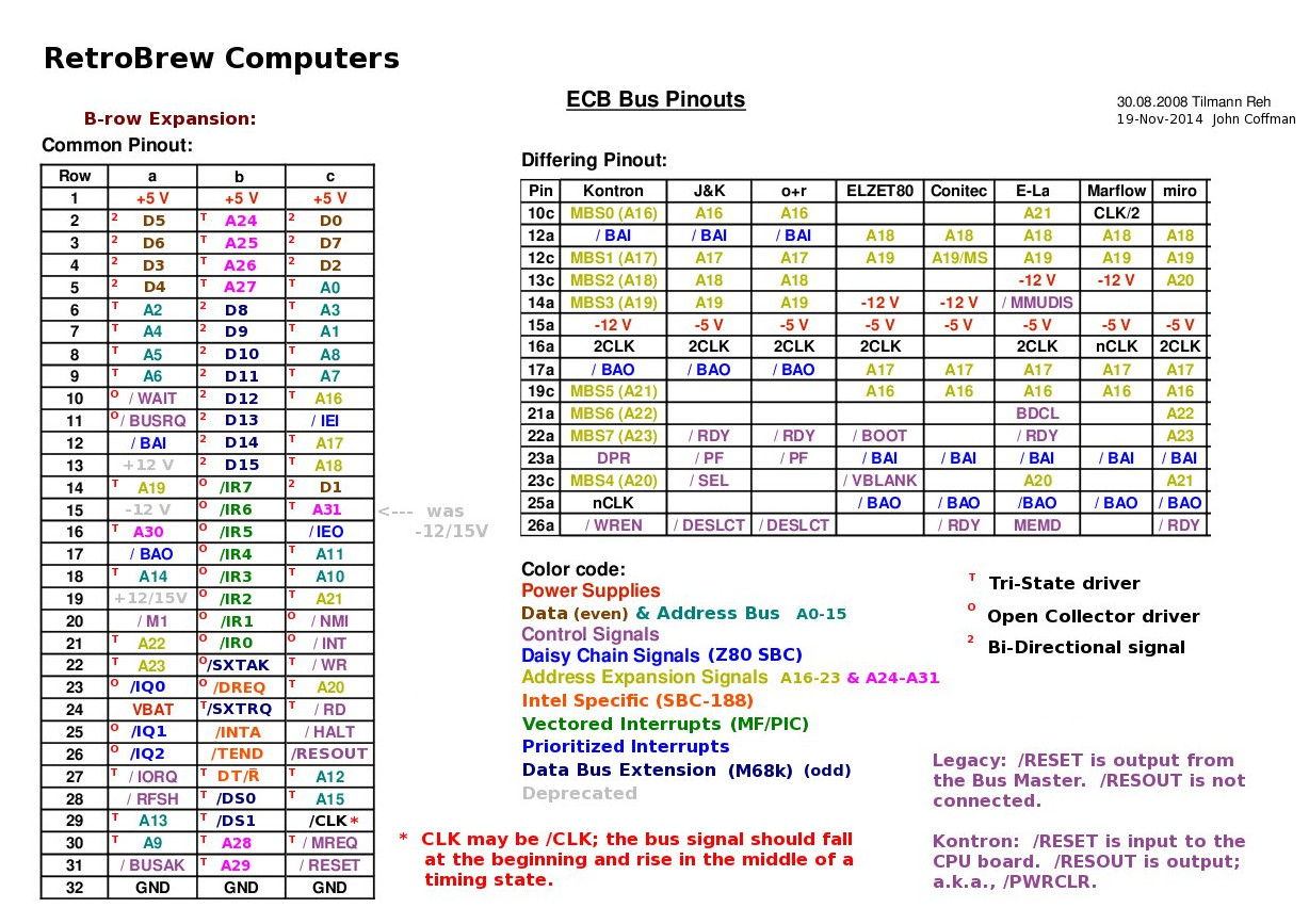
The German firm Kontron defined what is believed to be the earliest bus using the 96-pin DIN 41612 EuroCard connectors. The bus for their Z80 offering used only the A-row and C-row pins; the B-row was left entirely unused to allow for the use of 64-pin connectors in the 96-pin format.
The earliest known RetroBrew bus definition included B-row pin definitions to facilitate the anticipated expansion of the Z80 bus to other processors, particularly Intel. To this day, the ECB SBC v2 (Z80) does not use the B-row pins.
One error occurred in defining the first RetroBrew bus: confusion between signals RESET (C-31) and RESOUT (C-26). The error resulted in a bad guess at what Kontron's intentions were with these two signals. SBC v1 (Z80) used RESET as an output from the CPU board to peripheral boards and did not use the RESOUT signal at all. Peripheral boards were designed with this assumption. When it was pointed out several years ago (I am unsure of the date) that Kontron's intention was for RESET to be an input to the CPU board only and that the CPU board would then put out a signal, RESOUT, to all of the peripheral boards in the system.
The resolution to the above mistake is that all the newer CPU and peripheral boards have a reset selection jumper to select which RetroBrew reset convention is to be used. Look for a 3-pin jumper header: shorting pins 1-2 indicates the older, erroneous, reset convention for use with older boards; shorting pins 2-3 indicates the use of the Kontron convention. The Kontron convention is essential if RESET is to be received from any of the ECB backplanes, and only newer boards are allowed in such a system. Old CPU boards have a 2-pin Reset (in) connection as well as a reset switch right on the CPU card.
The 8253 Programmable Interval Timer (PIT) can be used as a baud rate generator for serial communication by generating clock pulses at the required frequency. This is done by programming one of its three counters to divide an input clock signal down to the desired baud rate.
Select the Counter: The 8253 has three counters (Counter 0, Counter 1, Counter 2). You need to choose one for generating the baud rate.
Provide the Clock Input:
The 8253 typically receives a clock input (e.g., 1.8432 MHz or some other standard clock frequency). Ensure the clock is stable and properly connected.
Calculate the Divider Value:
The baud rate is generated by dividing the input clock using a counter. The formula is:
Input Frequency RateDivider=Baud RateClock Input Frequency
For example, if the input clock is 1.8432 MHz and you need a baud rate of 9600, the divider value is:
1843200÷9600=192
Program the 8253:
Load the appropriate mode (typically Mode 2 – Rate Generator or Mode 3 – Square Wave).
Load the divider value into the selected counter.
Start the timer and route its output to the serial communication hardware (like 8251 USART or UART).
Connect Output to Serial Device: The output of the 8253 counter is connected to the baud rate clock input of a serial communication device like the 8251 USART or a UART module.
Use Counter 0 of 8253.
Program it in Mode 2 (Rate Generator).
Load 192 as the divider value.
Assembly code
    MOV AL, 34H    ; Control Word: Counter 0, Mode 2, LSB/MSB
    OUT 43H, AL    ; Send control word to 8253
    MOV AL, 192    ; Load LSB (Least Significant Byte)
    OUT 40H, AL    ; Send LSB to Counter 0
    MOV AL, 0      ; Load MSB (Most Significant Byte)
    OUT 40H, AL    ; Send MSB to Counter 0
43H → Control port of 8253
40H → Counter 0 data port
Mode 2 (Rate Generator) → Outputs a frequency suitable for baud generation.
Mode 3 (Square Wave Generator) → Outputs a symmetrical square wave (useful in some applications).
The OUT0 pin of 8253 (if using Counter 0) is connected to the clock input of 8251 USART or UART for serial communication.
Use Mode 2 (Rate Generator)
Compute the divider value using the formula
Program the control word and counter value
Connect output to the serial device clock input.
This setup allows the 8253 to act as a baud rate generator for serial communication.
As crystal frequency is 18.432 Mhz and it is outputted from I8224, we can use that frequency to generate baud rate clock signal for I8251. Below is the solution.
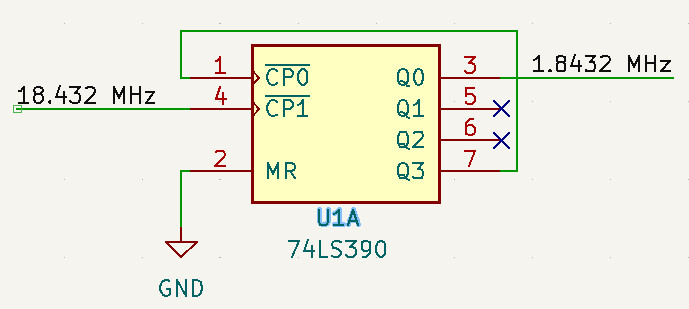
74LS390 contains two decade counters, where /CP0 → Q0 functions as a divider by 2, and /CP1 → Q1, Q2, Q3 operates as a divider by 5. We send an 18.432 MHz clock signal from I8224 to /CP1; it is divided by 5 and then fed to /CP0, where it is divided by 2. This arrangement will generate a square signal with an exact 50% duty cycle. The output signal from Q0 is then fed to the I8252 timer, where the appropriate baud rate can be generated.
In the picture below you can see shadow FLASH select logic schematics.
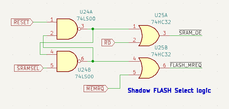
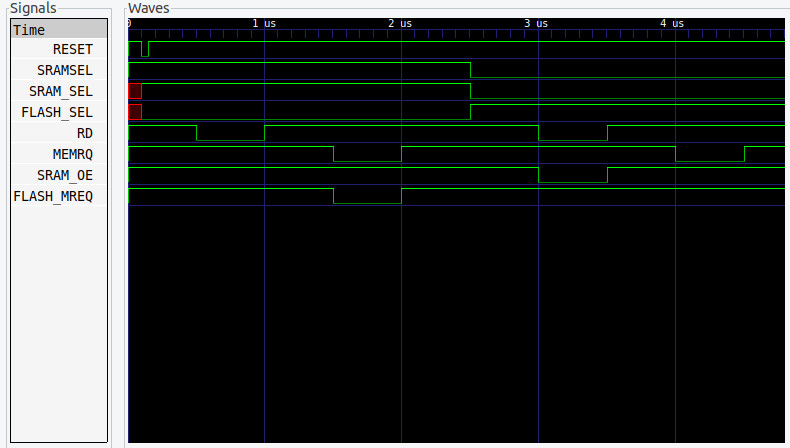
After /RESET (at this point, the /SRAMSELECT signal from the IO decoder is HIGH), /SRAM_SEL is HIGH and /FLASH_SEL is LOW. Now /SRAM_OE is HIGH (the DATA from RAM are in high impedance, although writing is not prohibited), so the /RD signal has no effect on /SRAM_OE. Only changes in /MEMRQ will impact the /FLASH_MREQ signal, which means that only FLASH memory can be accessed, either for reading or for writing. So it is also possible to flash the memory using a programmer connected to the ECB bus. A simulation has also been conducted in Verilog (via iVerilog) and can be seen below.
/*
 Test bench
*/

`timescale 10ns/10ns

module shadow_flash_select_logic_tb();

   reg MEMRQ, RESET, SRAMSEL, RD;
   wire SRAM_SEL, FLASH_SEL, SRAM_OE, FLASH_MEMRQ;

   initial begin
      $dumpfile ("shadow_flash_select_logic.vcd");
      $dumpvars;
   end

  initial begin
     RESET = 1;
     #10
     RESET = 0;
     #5
     RESET = 1;
  end
Simulation result in gtkwave is shown below.
As we also have to send and read data from the ECB bus, we have to make sure that bus data buffers are properly directed if there is a bus request (BUSRQ) from the bus itself.
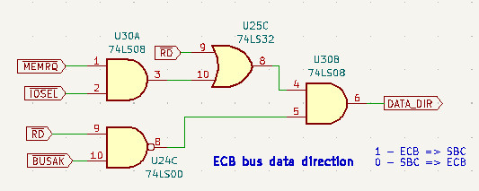
Signal DATA_DIR Select the direction of the data buffer. If DATA_DIR is log 0, data direction is from the board to the ECB bus, and if DATA_DIR is log 1, 1data can flow from the ECB bus to the board.
This is done by the circuit below. Basically, the upper part (/MEMRQ, /RD, /IOSEL, which is low when internal peripherals are selected) takes care of standard operations, and the upper part is involved when there is a request from the ECB bus. (/RD, /BUSAK)
Below you can see simulation code and simulation result.
/*
 Test bench
*/

`timescale 10ns/10ns

module shadow_flash_select_logic_tb();

   reg MREQ, IOSEL, RD, BUSAK;
   wire DATA_DIR, MREQ_IOSEL, RD_BUSAK, DATAEN;

   initial begin
      $dumpfile ("ecb_data_dir_logic.vcd");
      $dumpvars;
   end

  initial begin
    MREQ = 1;
    IOSEL = 1;
    RD = 1;
    BUSAK = 1;
/* MREQ and RD */
    #50
MREQ = 0;And the simulation result is below.

Internal peripherals are selected by the following decoder.
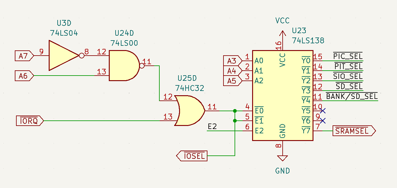
The address space with this circuit is 0x40 – 0x7f.
Where base addresses of peripherals are in the following table.
| Peripheral | Address range |
| PIC 8259A | 0x40 – 047 |
| PIT 8253 | 0x48 - 0x4F |
| SIO 8251 | 0x50 - 0x57 |
| RAM bank/ SD card select register (/BANK/SD_SEL ) | 0x58 - 0x5F |
| RAM select signal (/SRAMSEL) | 0x78 - 0x7F |
Below is verilog simulation result for the decoder.
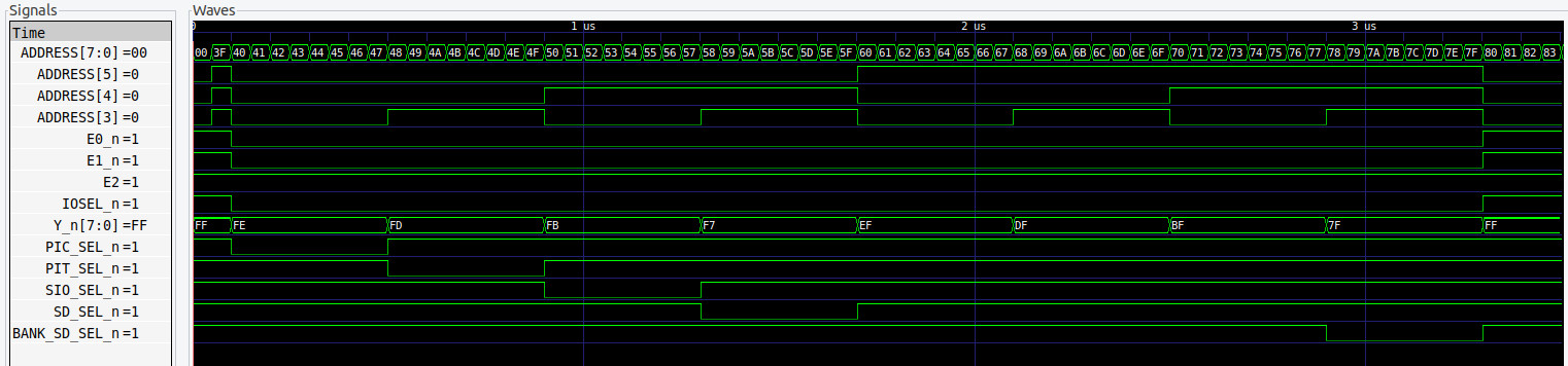
And the source code. I intentionally use primitives for simulation of 74LS138 to prevent some simulation glitches I got when I tried to use behavioral modeling. It is quite simplified as I’ve just wanted to verify address space for peripherals.
/*
 Test bench
*/

`timescale 10ns/10ns

module SN74LS138(input [2:0] ADDR, input E0_n, E1_n, E2, output wire [7:0] Y_n);

  not(E2_n, E2);
  nor(ENBL, E2_n, E0_n, E1_n);
  not(A_n, ADDR[0]);
  not(B_n, ADDR[1]);
  not(C_n, ADDR[2]);
  not(A, A_n);
  not(B, B_n);
  not(C, C_n);
  nand(Y_n[0], A_n, B_n, C_n, ENBL);
  nand(Y_n[1], A, B_n, C_n, ENBL);
  nand(Y_n[2], A_n, B, C_n, ENBL);
  nand(Y_n[3], A, B, C_n, ENBL);
  nand(Y_n[4], A_n, B_n, C, ENBL);
  nand(Y_n[5], A, B_n, C, ENBL);
  nand(Y_n[6], A_n, B, C, ENBL);
nand(Y_n[7], A, B, C, ENBL);| Qty | Value | Footprint | References |
|---|---|---|---|
| 31 | 0.1uF | Capacitor_THT:C_Disc_D4.3mm_W1.9mm_P5.00mm | C10, C11, C12, C13, C14, C15, C18, C20, C26, C27, C28, C29, C30, C31, C32, C33 +15 |
| 4 | 1.0 uF | Capacitor_THT:C_Rect_L7.2mm_W3.0mm_P5.00mm_FKS2_FKP2_MKS2_MKP2 | C22, C23, C24, C25 |
| 4 | Jumper_3_Bridged12 | Connector_PinHeader_2.54mm:PinHeader_1x03_P2.54mm_Vertical | JP2, JP3, JP4, JP6 |
| 3 | 1k5 | Resistor_THT:R_Axial_DIN0204_L3.6mm_D1.6mm_P7.62mm_Horizontal | R3, R7, R8 |
| 3 | 74LS245 | Package_DIP:DIP-20_W7.62mm_Socket | U11, U12, U14 |
| 2 | 1.0uF | Capacitor_THT:C_Disc_D4.7mm_W2.5mm_P5.00mm | C17, C19 |
| 2 | 10k | Resistor_THT:R_Axial_DIN0204_L3.6mm_D1.6mm_P7.62mm_Horizontal | R10, R11 |
| 2 | 220uF | Capacitor_THT:CP_Radial_D5.0mm_P2.00mm | C44, C45 |
| 2 | 470uF | Capacitor_THT:CP_Radial_D6.3mm_P2.50mm | C3, C5 |
| 2 | 74LS08 | Package_DIP:DIP-14_W7.62mm_Socket | U1, U30 |
| 2 | 74LS125 | Package_DIP:DIP-14_W7.62mm_Socket | U2, U6 |
| 2 | 74LS32 | Package_DIP:DIP-14_W7.62mm_Socket | U25, U27 |
| 1 | +5V/5A | 8080Board:694106301002_1 | J1 |
| 1 | +5VP | LED_THT:LED_D3.0mm | D3 |
| 1 | 0.01uF | Capacitor_THT:C_Disc_D3.0mm_W1.6mm_P2.50mm | C21 |
| 1 | 10 | Resistor_THT:R_Axial_DIN0204_L3.6mm_D1.6mm_P7.62mm_Horizontal | R2 |
| 1 | 100k | Resistor_THT:R_Axial_DIN0204_L3.6mm_D1.6mm_P7.62mm_Horizontal | R4 |
| 1 | 10k | Resistor_THT:R_Array_SIP5 | RN1 |
| 1 | 10k | Resistor_THT:R_Array_SIP8 | RN3 |
| 1 | 10k | Resistor_THT:R_Array_SIP9 | RN2 |
| 1 | 18,432MHz | Crystal:Crystal_HC49-U_Vertical | Y1 |
| 1 | 1N4148 | Diode_THT:D_DO-35_SOD27_P7.62mm_Horizontal | D1 |
| 1 | 1N5818 | Diode_THT:D_DO-41_SOD81_P10.16mm_Horizontal | D6 |
| 1 | 1k | Resistor_THT:R_Axial_DIN0204_L3.6mm_D1.6mm_P7.62mm_Horizontal | R6 |
| 1 | 220k | Resistor_THT:R_Axial_DIN0204_L3.6mm_D1.6mm_P7.62mm_Horizontal | R1 |
| 1 | 33 | Resistor_THT:R_Axial_DIN0204_L3.6mm_D1.6mm_P7.62mm_Horizontal | R5 |
| 1 | 33uF | Inductor_THT:L_Radial_D6.0mm_P4.00mm | L1 |
| 1 | 39p | Capacitor_THT:C_Disc_D5.0mm_W2.5mm_P2.50mm | C1 |
| 1 | 470 | Resistor_THT:R_Axial_DIN0204_L3.6mm_D1.6mm_P7.62mm_Horizontal | R9 |
| 1 | 47uF | Capacitor_THT:CP_Radial_D5.0mm_P2.00mm | C16 |
| 1 | 4u7 | Capacitor_THT:CP_Radial_D4.0mm_P1.50mm | C2 |
| 1 | 74HC374 | Package_DIP:DIP-20_W7.62mm_Socket | U22 |
| 1 | 74LS00 | Package_DIP:DIP-14_W7.62mm_Socket | U24 |
| 1 | 74LS04 | Package_DIP:DIP-14_W7.62mm_Socket | U3 |
| 1 | 74LS138 | Package_DIP:DIP-16_W7.62mm_Socket | U23 |
| 1 | 74LS240 | Package_DIP:DIP-20_W7.62mm_Socket | U16 |
| 1 | 74LS243 | Package_DIP:DIP-14_W7.62mm_Socket | U13 |
| 1 | 74LS244 | Package_DIP:DIP-20_W7.62mm_Socket | U15 |
| 1 | 74LS390 | Package_DIP:DIP-16_W7.62mm_Socket | U17 |
| 1 | 74LS74 | Package_DIP:DIP-14_W7.62mm_Socket | U4 |
| 1 | 8080A | Package_DIP:DIP-40_W15.24mm_Socket | U5 |
| 1 | 8224 | Package_DIP:DIP-16_W7.62mm_Socket | IC1 |
| 1 | 8228 | Package_DIP:DIP-28_W15.24mm_Socket | IC2 |
| 1 | 8251 | Package_DIP:DIP-28_W15.24mm_Socket | U20 |
| 1 | 8253 | Package_DIP:DIP-24_W15.24mm_Socket | U18 |
| 1 | 8259A | Package_DIP:DIP-28_W15.24mm_Socket | U19 |
| 1 | AS6C4008-55PCN | Package_DIP:DIP-32_W15.24mm_Socket | U28 |
| 1 | AT-1224-TWT-R | Buzzer_Beeper:MagneticBuzzer_ProSignal_ABT-410-RC | SP1 |
| 1 | Bank0/Bank1 | Connector_PinHeader_2.54mm:PinHeader_1x02_P2.54mm_Vertical | JP5 |
| 1 | C96ABC | Connector_DIN:DIN41612_C_3x32_Male_Horizontal_THT | U10 |
| 1 | Conn_01x07 | Connector_PinSocket_2.54mm:PinSocket_1x07_P2.54mm_Vertical | J3 |
| 1 | DISK | LED_THT:LED_D3.0mm | D4 |
| 1 | HALT | LED_THT:LED_D3.0mm | D2 |
| 1 | IRF4905LPBF | 8080Board:TO254P483X1016X1501-3P | Q1 |
| 1 | Jumper_3_Bridged23 | Connector_PinHeader_2.54mm:PinHeader_1x03_P2.54mm_Vertical | JP1 |
| 1 | LT1109A | Package_DIP:DIP-8_W7.62mm_Socket | U7 |
| 1 | MAX232 | Package_DIP:DIP-16_W7.62mm_Socket | U21 |
| 1 | PN2222A | Package_TO_SOT_THT:TO-92_Inline | Q2 |
| 1 | RESET | Connector_PinHeader_2.54mm:PinHeader_1x02_P2.54mm_Vertical | SW1 |
| 1 | RS232 | Connector_PinHeader_2.54mm:PinHeader_2x05_P2.54mm_Vertical | J4 |
| 1 | RUN | LED_THT:LED_D3.0mm | D5 |
| 1 | SPEAKER | Connector_PinHeader_2.54mm:PinHeader_1x04_P2.54mm_Vertical | J2 |
| 1 | SST39SF010 | Package_DIP:DIP-32_W15.24mm_Socket | U29 |
| 1 | TC7660H | Package_DIP:DIP-8_W7.62mm_Socket | U9 |
The 111 most common of 112 parts.
RichCini/LomasBoards
Small repository of files/data related to Lomas Data Products S-100 boards.


CPTforever/8088-MicroATX-Computer
A 8088 based, IBM 5150 like computer compatible with the MicroATX motherboard form factor.


lynchaj/duodyne
Duodyne is a hobbyist retrocomputer system designed to run ROMWBW. It is comprised of modules on a system bus


lynchaj/rhyophyre
Single Board Computer featuring Zilog Z180 processor and NEC µPD7220 Graphics Display Controller
It measures 160.5 × 100.2 mm and has 2 copper layers, 1.6 mm thick.
112 parts, built around the 74LS245SC, 74LS125DC, 74LS240DC and MAX232N. The full list of its parts is on this page, with links to each part's symbol and footprint where PCBKit's library has them.
From the sladek/SBC_8080_ECB repository on GitHub, at the commit this page was made from: the board is kicad/8080_ECB_SBC/8080_Board.kicad_pcb and its schematic kicad/8080_ECB_SBC/8080_Board.kicad_sch. PCBKit opens the board in the browser, with nothing to install.
Its repository states no licence, so its author keeps all rights: ask sladek before reusing the design.