4 layers170.1 × 170.1 mm

 skiselev/Z80-CPM5
RCBus Z80 CPU and Memory Module designed with discrete logic
Z80-cpu mem is an open-source printed circuit board by skiselev, from the skiselev/Z80-CPM repository on GitHub, published under the CERN-OHL-S-2.0 licence. It is a 2-layer board of 101.6 × 53.3 mm with 32 parts on 108 nets, routed with 1,514 tracks and 78 vias.
It is built around the 74AHCT32D, 74AHCT00D and 74AHCT138D, with the DS1233 among its other parts. Its parts include 11 capacitors, 9 ICs, 1 connector, 1 switch and 1 crystal. It belongs with the retro computing and games boards of this library.


RCBus Z80 CPU, 512 KiB SRAM, and 512 KiB Flash ROM module for RCBus systems designed using discrete logic
Z80-CPM is an RCBus and RC2014* compatible module, designed to run RomWBW firmware including CP/M, ZSDOS, and various applications under these OSes. Z80-CPM combines functionality of the following RC2014* modules on a single module, thus saving space on the backplane:
Minimal CP/M computer system can be built using Z80-CPM module, a backplane, and a serial port module, for example Steve Cousins' SC716 or SC725 Z80 SIO modules, or MC68B50 ACIA. A Compact Flash module can be added for additional storage. For a compact system, a 3-slot SC723 can be used.
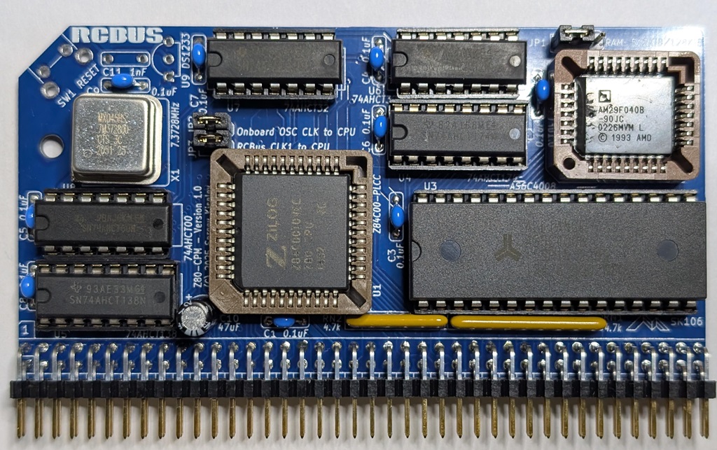
Please refer to Assembly Instructions document
Z80-CPM supports up to 512 KiB of RAM and up to 512 KiB of Flash ROM. It has a simple memory bank switching mechanism with two 32 KiB memory banks, inspired by Steve Cousin's SC602 Memory Module. This memory bank mechanism provides minimal required functionality for the RomWBW RCZ80_std.rom image to be used without any modifications. The upper 32 KiB bank is always mapped to the top 32 KiB of the physical RAM. The lower 32 KiB bank can be mapped to any 32 KiB size page in the physical memory. The memory page is selected by writting either 0x78 or 0x79 I/O ports, that are mapped to the same page select register.
| Port | Bit # | Function | Value |
|---|---|---|---|
| 0x78, 0x79 | 0 | Not implemented | Can be set to either 0 or 1 |
| 0x78, 0x79 | 5-1 | Page number for bank #0 0x0000-0xr7FFF | 0-31 - Page number |
| 0x78, 0x79 | 7-6 | Not implemented | Should be set to 0 |
| Jumper Position | Description |
|---|---|
| 1-2 | 512 KiB SRAM |
| 2-3 | 128 KiB SRAM |
| Jumper Position | Description |
|---|---|
| Closed | X1 oscillator is connected to the CPU |
| Open | X1 oscillator is not connected to the CPU |
| Jumper Position | Description |
|---|---|
| Closed | CLK1 signal is connected to the CPU |
| Open | CLK1 signal is not connected to the CPU |
The module supports the following options for the CPU clock:
| Pin | Signal Name | Description | Pin | Signal Name | Description |
|---|---|---|---|---|---|
| 1 | A15 | Address A15; Output | 41 | p41 | Reserved; Not connected |
| 2 | A14 | Address A14; Output | 42 | /BAI | Bus Acknowledge In; Not connected |
| 3 | A13 | Address A13; Output | 43 | /BAO | Bus Acknowledge Out; Not connected |
| 4 | A12 | Address A12; Output | 44 | p44 | Reserved; Not connected |
| 5 | A11 | Address A11; Output | 45 | p45 | Reserved; Not connected |
| 6 | A10 | Address A10; Output | 46 | p46 | Reserved; Not connected |
| 7 | A9 | Address A9; Output | 47 | p47 | Reserved; Not connected |
| 8 | A8 | Address A8; Output | 48 | p48 | Reserved; Not connected |
| 9 | A7 | Address A7; Output | 49 | A23 | Address A23; Not connected |
| 10 | A6 | Address A6; Output | 50 | A22 | Address A22; Not connected |
| 11 | A5 | Address A5; Output | 51 | A21 | Address A21; Not connected |
| 12 | A4 | Address A4; Output | 52 | A20 | Address A20; Not connected |
| 13 | A3 | Address A3; Output | 53 | A19 | Address A19; Output |
| 14 | A2 | Address A2; Output | 54 | A18 | Address A18; Output |
| 15 | A1 | Address A1; Output | 55 | A17 | Address A17; Output |
| 16 | A0 | Address A0; Output | 56 | A16 | Address A16; Output |
| 17 | GND | Ground | 57 | GND | Ground |
| 18 | VCC | Power Supply - +5V | 58 | VCC | Power Supply - +5V |
| 19 | /M1 | Machine Cycle One; Output | 59 | /RFSH | DRAM refresh; Output |
| 20 | /RESET | Reset; Output | 60 | PAGE | Page ROM/RAM input; Not connected |
| 21 | CLK1 | CPU Clock; Output | 61 | CLK2 | UART Clock; Not connected |
| 22 | /INT | Interrupt; Input | 62 | /BUSACK | DMA Bus Acknowledge; Output |
| 23 | /MREQ | Memory Request; Output | 63 | /HALT | Halt; Output |
| 24 | /WR | Write Request; Output | 64 | /BUSREQ | DMA Bus Request; Input |
| 25 | /RD | Read Request; Output | 65 | /WAIT | Wait; Input |
| 26 | /IORQ | Input/Output Request; Output | 66 | /NMI | Non-maskable Interrupt; Input |
| 27 | D0 | Data D0; Input/Output | 67 | D8 | Data D8; Input/Output; Not connected |
| 28 | D1 | Data D1; Input/Output | 68 | D9 | Data D9; Input/Output; Not connected |
| 29 | D2 | Data D2; Input/Output | 69 | D10 | Data D10; Input/Output; Not connected |
| 30 | D3 | Data D3; Input/Output | 70 | D11 | Data D11; Input/Output; Not connected |
| 31 | D4 | Data D4; Input/Output | 71 | D12 | Data D12; Input/Output; Not connected |
| 32 | D5 | Data D5; Input/Output | 72 | D13 | Data D13; Input/Output; Not connected |
| 33 | D6 | Data D6; Input/Output | 73 | D14 | Data D14; Input/Output; Not connected |
| 34 | D7 | Data D7; Input/Output | 74 | D15 | Data D15; Input/Output; Not connected |
| 35 | TX | Channel 1, Transmit Data; Not Connected | 75 | TX2 | Channel 2, Transmit Data; Not Connected |
| 36 | RX | Channel 1, Receive Data; Not Connected | 76 | RX2 | Channel 2, Receive Data; Not Connected |
| 37 | /IRQ1 | Interrupt Request 1; Not connected | 77 | /IRQ2 | Interrupt Request 2; Not connected |
| 38 | IEI | Interrupt Enable In; Not connected | 78 | p78 | Reserved; Not connected |
| 39 | IEO | Interrupt Enable Out; Not connected | 79 | p79 | Reserved; Not connected |
| 40 | USER4 | User Pin 4; Not connected | 80 | USER8 | User Pin 8; Not connected |
Mouser projects - All components except of the PCB and the CPU:
Z80-CPM project on Tindie:
| Component type | Reference | Description | Quantity | Possible sources and notes |
|---|---|---|---|---|
| PCB | Z80-CPM PCB - Version 1.0 | 1 | Buy from my Tindie store: Complete kit; Z80-CPM PCB, or order from a PCB manufacturer of your choice using provided Gerber or KiCad files | |
| Integrated Circuit | U1 | Z84C00xxVEG - Z80 CPU, CMOS, 44 pin PLCC | 1 | Mouser 692-Z84C0010VEG |
| Integrated Circuit | U2 | SST39SF040 - 512 KiB Flash ROM, 32 pin PLCC | 1 | Mouser 804-39SF0407CNHE |
| Integrated Circuit | U3 | AS6C4008 - 512 KiB SRAM, 32 pin DIP | 1 | Mouser 913-AS6C4008-55PCN |
| Integrated Circuit | U4 | 74AHCT174 - Hex D-Type Flip Flop, 16 pin DIP | 1 | Mouser 595-SN74AHCT174N |
| Integrated Circuit | U5 | 74HCT138 - 3-to-8 Decoder, 16 pin DIP | 1 | Mouser 595-CD74HCT138E |
| Integrated Circuit | U6, U7 | 74AHCT32 - Quad 2-Input OR Gate, 14 pin DIP | 2 | Mouser 595-SN74AHCT32N |
| Integrated Circuit | U8 | 74AHCT00 - Quad 2-Input NAND Gate, 14 pin DIP | 1 | Mouser 595-SN74AHCT00N |
| Integrated Circuit | U9 | DS1233-5 - CPU Supervisor, 5V, TO-92-3 | 1 | Mouser 700-DS1233-5. Note U9 is an optional on-board CPU supervisor. |
| Oscillator | X1 | 7.3728 MHz, CMOS oscillator, half can | 1 | Mouser 774-MXO45HS-3C-7.3 or 520-2200B-073 |
| Pin Header | J1 | 40x2 pin header, 2.54 mm pitch, right angle | 1 | Mouser 737-PH2RA-80-UA, 517-5121TG |
| Pin Header | JP1 | 3x1 pin header, 2.54 mm pitch, vertical | 1 | Mouser 649-68000-203HLF. |
| Pin Header | JP2, JP3 | 2x2 pin header, 2.54 mm pitch, vertical | 1 | Mouser 649-67996-104HLF. |
| Jumper | JP1 - JP3 | Shunt, 2 pin 2.54 mm pitch | 3 | Mouser 806-SX1100-B. |
| Tactile switch | SW1 | Tactile switch, 6 mm, right angle | 1 | Mouser 653-B3F-3152. SW1 is an optional reset switch. |
| Capacitor | C1 - C9 | 0.1 uF, 50V, MLCC, 5 mm pitch | 9 | Mouser 594-K104K15X7RF53H5. |
| Capacitor | C10 | 47 uF, 25V, electrolytic, 5 x 11 mm, 2 mm pitch | 1 | Mouser 667-EEU-FR1E470 |
| Capacitor | C11 | 1 nF, 50V, MLCC, 5 mm pitch | 1 | Mouser 594-K102K15X7RF5TH5. Note: C11 is optional, required if U9 installed and manual reset functionality is desired. |
| Resistor Array | RN1 | 4.7 kohm, bussed, 9 pin SIP | 1 | Mouser 652-4609X-1LF-4.7K or 652-4609X-AP1-472LF |
| Resistor Array | RN2 | 4.7 kohm, bussed, 6 pin SIP | 1 | Mouser 652-4606X-1LF-4.7K or 652-4606X-AP1-472LF |
| IC Socket | U1 | 44 pin PLCC, through hole | 1 | Mouser 737-PLCC-44-AT, 517-8444-11B1-RK-TP |
| IC Socket | U2 | 32 pin PLCC, through hole | 1 | Mouser 737-PLCC-32-AT, 517-8432-11B1-RK-TP |
| IC Socket | U3 | 32 pin DIP | 1 | Mouser 737-ICS-632-T, 517-4832-6000-CP |
| IC Socket | U4, U5 | 16 pin DIP | 2 | Mouser 737-ICS-316-T, 517-4816-3000-CP. |
| IC Socket | U6 - U8 | 14 pin DIP | 3 | Mouser 737-ICS-314-T, 517-4816-3000-CP. |
| Oscillator Socket | X1 | 4 pin DIP, Half Can | 1 | Mouser 535-1108800 |
Version 1.1
Version 1.0
Z80-CPM is an open source hardware project. The hardware design itself, including schematic and PCB layout design files are licensed under the strongly-reciprocal variant of CERN Open Hardware Licence version 2. Documentation, including this file, is licensed under the Creative Commons Attribution-ShareAlike 4.0 International License.
| Qty | Value | Footprint | References |
|---|---|---|---|
| 9 | 0.1uF | My_Components:Cap_Cer_508 | C1, C2, C3, C4, C5, C6, C7, C8, C9 |
| 2 | 74AHCT32 | My_Components:IC_DIP14_300 | U6, U7 |
| 1 | 1nF | My_Components:Cap_Cer_508 | C11 |
| 1 | 4.7k | My_Components:Conn_SIL9 | RN1 |
| 1 | 4.7k | My_Components:Conn_SIL6 | RN2 |
| 1 | 47uF | My_Components:Cap_Elec_Radial_5mm | C10 |
| 1 | 7.3728MHz | My_Components:OSC_Half_Can_DIP8 | X1 |
| 1 | 74AHCT00 | My_Components:IC_DIP14_300 | U8 |
| 1 | 74AHCT138 | My_Components:IC_DIP16_300 | U5 |
| 1 | 74AHCT174 | My_Components:IC_DIP16_300 | U4 |
| 1 | AS6C4008 | My_Components:IC_DIP32_600 | U3 |
| 1 | DS1233 | My_Components:Transistor_TO92_EBC_254 | U9 |
| 1 | Logo_Open_Hardware_Large | Symbol:OSHW-Logo2_7.3x6mm_SilkScreen | LOGO1 |
| 1 | M3 | MountingHole:MountingHole_3.2mm_M3_DIN965 | H1 |
| 1 | Onboard OSC CLK to CPU | My_Components:Conn_Pin_Header_2x1_2.54mm | JP2 |
| 1 | RAM: 512KiB/128KiB | My_Components:Conn_Pin_Header_3x1_2.54mm | JP1 |
| 1 | RCBUS_Logo | My_Components:RCBUS_Logo | LOGO2 |
| 1 | RCBus | My_Components:Conn_Pin_Header_40x2_2.54mm_Right_Angle_RCBus80 | J1 |
| 1 | RCBus CLK1 to CPU | My_Components:Conn_Pin_Header_2x1_2.54mm | JP3 |
| 1 | RESET | My_Components:Switch_Tactile_6mm_Right | SW1 |
| 1 | SST39SF040 | My_Components:IC_PLCC32_TH | U2 |
| 1 | Z84C00-PLCC | My_Components:IC_PLCC44_TH | U1 |
The 31 most common of 32 parts.

flypie/Ace-2019
Reimplimentation of the Jupiter ACE with slightly more modern hardware. https://www.jupiter-ace.co.uk/ the KiCad versions are the up to date designs which are available at https://jupiterdeuce.blogspot.com and…

punkfab/pcb-corpus
235 real KiCad boards from open-source hardware repositories, prepared as a placement and routing benchmark


RobertPHeller/RPi-RRCircuits
A collection of circuit designs for various MCUs, not just Raspberry Pis relating to Model Railroading

mikelawrence/esphome-rgbcct-led-controller
ESPHome RGBCCT LED Controller is a PCB design that support a 5-Channel LED arrangement with Red, Green, Blue, Warm White and Cool White LEDs.
It measures 101.6 × 53.3 mm and has 2 copper layers, 1.6 mm thick.
32 parts, built around the 74AHCT32D, 74AHCT00D, 74AHCT138D and DS1233. The full list of its parts is on this page, with links to each part's symbol and footprint where PCBKit's library has them.
From the skiselev/Z80-CPM repository on GitHub, at the commit this page was made from: the board is KiCad/z80-cpu-mem.kicad_pcb and its schematic KiCad/z80-cpu-mem.kicad_sch. PCBKit opens the board in the browser, with nothing to install.
Its repository publishes it under the CERN-OHL-S-2.0 licence: you may reuse it on that licence's terms (keep the author's notice, and for a copyleft licence share your changes alike).