
2 layers52.2 × 52.2 mm
Base promicro
google/mozc-devices
Circuit diagrams and firmware source code for Gboard DIY keyboards
30 parts3kApache-2.0

 skiselev/Z80-512K43
Z80 CPU and Memory Module
Z80-512K is an open-source printed circuit board by skiselev, from the skiselev/Z80-512K repository on GitHub. It is a 2-layer board of 101.6 × 53.3 mm with 30 parts on 107 nets, routed with 1,693 tracks and 81 vias.
It is built around the ADM693ANZ. Its parts include 7 capacitors, 7 resistors, 5 ICs, 3 connectors and 1 diode. It belongs with the retro computing and games boards and the FPGA and CPLD boards of this library.
Z80 CPU, 512 KiB SRAM, and 512 KiB Flash ROM module for RCBus systems
Z80-512K is an RCBus and RC2014* compatible module, designed to run RomWBW firmware including CP/M, ZSDOS, and various applications under these OSes. Z80-512K combines functionality of the following RC2014* modules on a single module, thus saving space on the backplane:
In addition to these functions, Z80-512K includes programmable CLK2 clock divider, support for battery-backed SRAM, power failure NMI generation, and a watchdog.
Minimal CP/M computer system can be built using Z80-512K module, a backplane, and a serial port module, such as Z80 SIO or MC68B50 ACIA. For configurable baud rate settings, it is recommened to use serial modules that can use CLK2 as a clock, for example Steve Cousins' SC716 or SC725 modules. Additional storage module is not required, since RomWBW utilizes part of ROM and SRAM for ROM and RAM disks respecitvely, but a Compact Flash module can be added for additional storage. For a compact system, a 3-slot SC723 can be used.
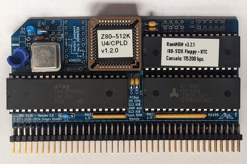
Please refer to Assembly Instructions document
Z80-512K uses an Atmel* ATF1504AS CPLD (complex programmable logic device) to implement Zeta SBC V2 compatible memory pager, watchdog control, and UART clock divider. These functions are configured using registers that are accessible using I/O ports. Upon reset, the configuration registers are set to values that result in an RC2014 compatible configuration, so that RomWBW RCZ80_std.rom image can be used without any modifications.
The following I/O ports are implemented in the CPLD:
Bits 0-4 define the ratio the 7.3728 MHz CPU clock (CLK1) is divided by to produce UART clock (CLK2). The output clock can be calculated using the following formula: fCLK2 (Hz) = 7372800 / (3m * 2n), where m is bit 4 of CONFIG register (0 or 1), and n are bits 3-0 of CONFIG register (0 to 15)
| Port | Bit # | Function | Value = 0 | Value = 1 |
|---|---|---|---|---|
| 0x6D | 0 | Divide CPU clock by 2 | Disable divide by 2 | Enable divide by 2 |
| 0x6D | 1 | Divide CPU clock by 4 | Disable divide by 4 | Enable divide by 4 |
| 0x6D | 2 | Divide CPU clock by 16 | Disable divide by 16 | Enable divide by 16 |
| 0x6D | 3 | Divide CPU clock by 256 | Disable divide by 256 | Enable divide by 256 |
| 0x6D | 4 | Divide CPU clock by 3 | Disable divide by 3 | Enable divide by 3 |
Bit 5 enables or disables the watchdog and controls the generation of watchdog (WDOG) signal. On the board the WDOG signal is connected to the CPU supervisor IC U5 ADM693A. The CPU supervisor will reset the board if WDOG signal is not pulsed within 1.6 seconds. When watchdog is disabled, the /M1 signal is routed to WDOG signal, so that it is pulsed on every instruction fetch. When watchdog is enabled, the WDOG signal should be pulsed by writting to WDOG register, port 0x6F (see below) in intervals of less than 1.6 seconds.
| Port | Bit # | Function | Value = 0 | Value = 1 |
|---|---|---|---|---|
| 0x6D | 5 | Watchdog enable | Disable watchdog | Enable watchdog |
| Port | Bit # | Function | Value |
|---|---|---|---|
| 0x6D | 7-6 | Not implemented | Should be set to 0 |
Any write to this port pulses the WDOG signal, which resets the watchdog in the CPU supervisor U5
| Port | Bit # | Function | Value |
|---|---|---|---|
| 0x6F | N/A | WDOG - Reset watchdog | Any write to this port resets the watchdog |
| Port | Bit # | Function | Value |
|---|---|---|---|
| 0x78 | 5-0 | MPGSEL_0 - Page number for bank #0 0x0000-0x3FFF | 0-31 - Page number |
| 0x78 | 7-6 | Not implemented | Should be set to 0 |
| 0x79 | 5-0 | MPGSEL_1 - Page number for bank #1 0x4000-0x7FFF | 0-31 - Page number |
| 0x79 | 7-6 | Not implemented | Should be set to 0 |
| 0x7A | 5-0 | MPGSEL_2 - Page number for bank #2 0x8000-0xBFFF | 0-31 - Page number |
| 0x7A | 7-6 | Not implemented | Should be set to 0 |
| 0x7B | 5-0 | MPGSEL_2 - Page number for bank #3 0xC000-0xFFFF | 0-31 - Page number |
| 0x7B | 7-6 | Not implemented | Should be set to 0 |
| Port | Bit # | Function | Value = 0 | Value = 1 |
|---|---|---|---|---|
| 0x7C | 0 | Memory paging enable | Disable memory paging | Enable memory paging |
| Port | Bit # | Function | Value |
|---|---|---|---|
| 0x7C | 7-1 | Not implemented | Should be set to 0 |
Connect 3V battery for SRAM backup to this connector.
Important: If the SRAM battery backup is not desired, short J1 with a jumper. Do not leave this connector open.
| Pin | Signal Name | Description |
|---|---|---|
| 1 | VBAT | Positive terminal - +3V |
| 2 | GND | Negative terminal - ground |
This connector can be used to program the U4 CPLD
| Pin | Signal Name | Description | Pin | Signal Name | Description |
|---|---|---|---|---|---|
| 1 | TCK | Test Clock | 2 | GND | Ground |
| 3 | TDO | Test Data Output | 4 | 5V | 5V Power Supply - Output to JTAG adapter |
| 5 | TMS | Test Mode Select | 6 | NC | No Connect |
| 7 | NC | No Connect | 8 | NC | No Connect |
| 9 | TDI | Test Data Input | 10 | GND | Ground |
| Pin | Signal Name | Description | Pin | Signal Name | Description |
|---|---|---|---|---|---|
| J3-1 | A15 | Address A15; Output | J3-41 | p41 | Reserved; Not connected |
| J3-2 | A14 | Address A14; Output | J3-42 | /BAI | Bus Acknowledge In; Not connected |
| J3-3 | A13 | Address A13; Output | J3-43 | /BAO | Bus Acknowledge Out; Not connected |
| J3-4 | A12 | Address A12; Output | J3-44 | p44 | Reserved; Not connected |
| J3-5 | A11 | Address A11; Output | J3-45 | p45 | Reserved; Not connected |
| J3-6 | A10 | Address A10; Output | J3-46 | p46 | Reserved; Not connected |
| J3-7 | A9 | Address A9; Output | J3-47 | p47 | Reserved; Not connected |
| J3-8 | A8 | Address A8; Output | J3-48 | p48 | Reserved; Not connected |
| J3-9 | A7 | Address A7; Output | J3-49 | A23 | Address A23; Input; Not connected |
| J3-10 | A6 | Address A6; Output | J3-50 | A22 | Address A22; Input; Not connected |
| J3-11 | A5 | Address A5; Output | J3-51 | A21 | Address A21; Input; Not connected |
| J3-12 | A4 | Address A4; Output | J3-52 | A20 | Address A20; Input; Not connected |
| J3-13 | A3 | Address A3; Output | J3-53 | A19 | Address A19; Input; Not connected |
| J3-14 | A2 | Address A2; Output | J3-54 | A18 | Address A18; Input; Not connected |
| J3-15 | A1 | Address A1; Output | J3-55 | A17 | Address A17; Input; Not connected |
| J3-16 | A0 | Address A0; Output | J3-56 | A16 | Address A16; Input; Not connected |
| J3-17 | GND | Ground | J3-57 | GND | Ground |
| J3-18 | VCC | Power Supply - +5V | J3-58 | VCC | Power Supply - +5V |
| J3-19 | /M1 | Machine Cycle One; Output | J3-59 | /RFSH | DRAM refresh; Output |
| J3-20 | /RESET | Reset; Output | J3-60 | PAGE | Page ROM/RAM input; Not connected |
| J3-21 | CLK1 | CPU Clock; Output | J3-61 | CLK2 | UART Clock (programmable); Output |
| J3-22 | /INT | Interrupt; Input | J3-62 | /BUSACK | DMA Bus Acknowledge; Output |
| J3-23 | /MREQ | Memory Request; Output | J3-63 | /HALT | Halt; Output |
| J3-24 | /WR | Write Request; Output | J3-64 | /BUSREQ | DMA Bus Request; Input |
| J3-25 | /RD | Read Request; Output | J3-65 | /WAIT | Wait; Input |
| J3-26 | /IORQ | Input/Output Request; Output | J3-66 | /NMI | Non-maskable Interrupt; Input |
| J3-27 | D0 | Data D0; Input/Output | J3-67 | D8 | Data D8; Input/Output; Not connected |
| J3-28 | D1 | Data D1; Input/Output | J3-68 | D9 | Data D9; Input/Output; Not connected |
| J3-29 | D2 | Data D2; Input/Output | J3-69 | D10 | Data D10; Input/Output; Not connected |
| J3-30 | D3 | Data D3; Input/Output | J3-70 | D11 | Data D11; Input/Output; Not connected |
| J3-31 | D4 | Data D4; Input/Output | J3-71 | D12 | Data D12; Input/Output; Not connected |
| J3-32 | D5 | Data D5; Input/Output | J3-72 | D13 | Data D13; Input/Output; Not connected |
| J3-33 | D6 | Data D6; Input/Output | J3-73 | D14 | Data D14; Input/Output; Not connected |
| J3-34 | D7 | Data D7; Input/Output | J3-74 | D15 | Data D15; Input/Output; Not connected |
| J3-35 | TX | Channel 1, Transmit Data; Not Connected | J3-75 | TX2 | Channel 2, Transmit Data; Not Connected |
| J3-36 | RX | Channel 1, Receive Data; Not Connected | J3-76 | RX2 | Channel 2, Receive Data; Not Connected |
| J3-37 | /IRQ1 | Interrupt Request 1; Not connected | J3-77 | /IRQ2 | Interrupt Request 2; Not connected |
| J3-38 | IEI | Interrupt Enable In; Not connected | J3-78 | p78 | Reserved; Not connected |
| J3-39 | IEO | Interrupt Enable Out; Not connected | J3-79 | p79 | Reserved; Not connected |
| J3-40 | USER4 | User Pin 4; Not connected | J3-80 | USER8 | User Pin 8; Not connected |
Mouser projects - all components except of the PCB:
Z80-512K project on Tindie:
| Component type | Reference | Description | Quantity | Possible sources and notes |
|---|---|---|---|---|
| PCB | Z80-512K PCB - Version 2.0 | 1 | Buy from my Tindie store: Complete kit; Z80-512K PCB, a preprogrammed CPLD and optionally a Flash ROM, or order from a PCB manufacturer of your choice using provided Gerber or KiCad files | |
| Integrated Circuit | U1 | Z84C00xxPEG - Z80 CPU, CMOS, 40 pin DIP | 1 | Mouser 692-Z84C0010PEG |
| Integrated Circuit | U2 | SST39SF040 - 512 KiB Flash ROM, 32 pin DIP | 1 | Mouser 804-39SF0407CPHE |
| Integrated Circuit | U3 | AS6C4008 - 512 KiB SRAM, 32 pin DIP | 1 | Mouser 913-AS6C4008-55PCN |
| Integrated Circuit | U4 | ATF1504AS - CPLD, 64 macrocells, 44 pin PLCC | 1 | Mouser 556-AF1504AS10JU44; Possible alternative: Altera EPM7064SLC44-10 |
| Integrated Circuit | U5 | ADM693A - Microprocessor Supervisory Circuit | 1 | Mouser 584-ADM693ANZ. Optional: CPU reset, watchdog, and power failure NMI. Possible alternatives: MAX693, LTC693, ADM691, MAX691, LTC691, ADM695, MAX695, LTC965, LTC1235 |
| Oscillator | X1 | 7.3728 MHz, CMOS oscillator, half can | 1 | Mouser 774-MXO45HS-3C-7.3 or 520-2200B-073 |
| LED | D1 | LED indicator, 3 mm, blue | 1 | Mouser 710-151033BS03000 |
| Connector | J1 | 2 pin header with friction lock, right angle | 1 | Mouser 571-6404572. Optional: battery-backed SRAM |
| Pin Header | J2 | 2x5 pin header, 2.54 mm pitch, vertical | 1 | Mouser 649-77313-118-10LF. Optional: JTAG header |
| Pin Header | J3 | 2x40 pin header, 2.54 mm pitch, right angle | 1 | Mouser 517-5121TG |
| Capacitor | C1 | 10 uF, 25V, MLCC, 5 mm pitch | 1 | Mouser 810-FG28X5R1E106MR06 |
| Capacitor | C2 - C7 | 0.1 uF, 50V, MLCC, 5 mm pitch | 6 | Mouser 594-K104K15X7RF53H5. Note: C5 is optional, required if U5 installed |
| Resistor Array | RN1 | 4.7 kohm, bussed, 9 pin SIP | 1 | Mouser 652-4609X-1LF-4.7K or 652-4609X-AP1-472LF |
| Resistor Array | RN2 | 4.7 kohm, bussed, 6 pin SIP | 1 | Mouser 652-4606X-1LF-4.7K or 652-4606X-AP1-472LF |
| Resistor | R1 - R5 | 10 kohm, 0.25 W, 1% tolerance, axial | 5 | Mouser 603-MFR-25FRF5210K. Optional: R1 - R4 - JTAG header, R5 - Power failure NMI |
| Resistor | R6 | 29.4 kohm, 0.25 W, 1% tolerance, axial | 1 | Mouser 603-MFR-25FBF52-29K4. Optional: Power failure NMI |
| Resistor | R7 | 1 kohm, 0.25 W, axial | 1 | Mouser 603-MFR-25FRF521K |
| Trimmer Resistor | RV1 | 2 kohm, through hole | 1 | Mouser 652-3362W-1-202LF. Optional: Power failure NMI |
| IC Socket | U1 | 40 pin DIP | 1 | Mouser 517-4840-6000-CP |
| IC Socket | U2, U3 | 32 pin DIP | 2 | Mouser 517-4832-6000-CP |
| IC Socket | U4 | 44 pin PLCC, through hole | 1 | Mouser 517-8444-11B1-RK-TP |
| IC Socket | U5 | 16 pin DIP | 1 | Mouser 517-4816-3000-CP. Optional: CPU reset, watchdog, and power failure NMI. Install two wire jumpers as indicated on the PCB if U5 is not used. |
| Oscillator Socket | X1 | 4 pin DIP, Half Can | 1 | Mouser 535-1108800 |
| Jumper | J1 | Shunt, 2 pin 2.54 mm pitch | 1 | Mouser 806-SX1100-B. Optional: install if battery is not used, but U5 is installed |
| Connector Contacts | J1 | Connector contact | 2 | Mouser 571-14453361. Optional: connector for battery enclosure, install for battery-backed SRAM |
| Connector Housing | J1 | 2 pin housing, 2.54 mm pitch | 1 | Mouser 571-13758202. Optional: connector for battery enclosure, install for battery-backed SRAM |
| Battery holder | J1 | 2xAAA battery enclosure with switch | 1 | Mouser 12BH421/CS-GR. Optional: battery enclosure, install for battery-backed SRAM |
Z80-512K uses Atmel ATF1504AS or Intel*/Altera* EPM7064STC44 CPLD (U4) CPLD for memory pager and varous other logic. Atmel CPLD fuse map, Altera CPLD fuse map, and the CPLD source code are provided in CPLD directory of this repository. Use ATMISP software to program Atmel CPLD. Use free Altera Quartus II 13.0sp1 Web Edition to program Altera CPLD. Newer Quartus versions do not support Altera MAX7000 CPLDs.
Version 2.0:
Version 1.2
Version 1.1
Version 1.0
Version 1.1
Version 1.0
Z80-512K is an open source hardware project certified by Open Source Hardware Association, certification UID is US001061. The hardware design itself, including schematic and PCB layout design files are licensed under the strongly-reciprocal variant of CERN Open Hardware Licence version 2. The CPLD VHDL code is licensed under GNU General Public License v3. Documentation, including this file, is licensed under the Creative Commons Attribution-ShareAlike 4.0 International License.
| Qty | Value | Footprint | References |
|---|---|---|---|
| 6 | 100nF | My_Components:Cap_Cer_508 | C2, C3, C4, C5, C6, C7 |
| 5 | 10k | Resistor_THT:R_Axial_DIN0204_L3.6mm_D1.6mm_P2.54mm_Vertical | R1, R2, R3, R4, R5 |
| 1 | 10uF | My_Components:Cap_Cer_508 | C1 |
| 1 | 1k | Resistor_THT:R_Axial_DIN0204_L3.6mm_D1.6mm_P2.54mm_Vertical | R7 |
| 1 | 29.4k | Resistor_THT:R_Axial_DIN0204_L3.6mm_D1.6mm_P2.54mm_Vertical | R6 |
| 1 | 2k | Potentiometer_THT:Potentiometer_Bourns_3266W_Vertical | RV1 |
| 1 | 3.2mm | MountingHole:MountingHole_3.2mm_M3_DIN965 | H1 |
| 1 | 4.7k | My_Components:Conn_SIL9 | RN1 |
| 1 | 4.7k | My_Components:Conn_SIL6 | RN2 |
| 1 | 7.3728MHz | My_Components:OSC_Half_Can_DIP8 | X1 |
| 1 | ADM693A | My_Components:Socket_DIP16_300 | U5 |
| 1 | AS6C4008 | My_Components:Socket_DIP32_600 | U3 |
| 1 | ATF1504AS | My_Components:IC_PLCC44_TH | U4 |
| 1 | CPU | My_Components:LED_3mm | D1 |
| 1 | JTAG | My_Components:Conn_Pin_Header_5x2_2.54mm | J2 |
| 1 | Logo_Open_Hardware_Small | Symbol:OSHW-Logo_5.7x6mm_SilkScreen | LOGO1 |
| 1 | RCBus-80 | My_Components:Conn_Pin_Header_40x2_2.54mm_Right_Angle_RCBus80 | J3 |
| 1 | SST39SF040 | My_Components:Socket_DIP32_600 | U2 |
| 1 | VBAT | Connector_PinHeader_2.54mm:PinHeader_1x02_P2.54mm_Horizontal | J1 |
| 1 | Z84C00 | My_Components:Socket_DIP40_600 | U1 |
The 29 most common of 30 parts.
google/mozc-devices
Circuit diagrams and firmware source code for Gboard DIY keyboards


VoronDesign/Voron-Hardware
Cool Hardware designed by the Voron Design group

hoglet67/RGBtoHDMI
Bare-metal Raspberry Pi project that provides pixel-perfect sampling of Retro Computer RGB/YUV video and conversion to HDMI

tenderlove/initial-v
It's a BMW shifter converted to a Bluetooth Keyboard that you use with Vim

hackclub/OnBoard
💡 Join 1,000 teenagers and make your first PCB with a $100 grant!


It measures 101.6 × 53.3 mm and has 2 copper layers, 1.6 mm thick.
30 parts, built around the ADM693ANZ. The full list of its parts is on this page, with links to each part's symbol and footprint where PCBKit's library has them.
From the skiselev/Z80-512K repository on GitHub, at the commit this page was made from: the board is KiCad/Z80-512K.kicad_pcb and its schematic KiCad/Z80-512K.kicad_sch. PCBKit opens the board in the browser, with nothing to install.
Its repository states no licence, so its author keeps all rights: ask skiselev before reusing the design.