2 layers142.5 × 106.4 mm

 skarrmann/umbra13
24 key ergonomic keyboard with self-encasing PCB.
Umbra choc is an open-source printed circuit board by skarrmann, from the skarrmann/umbra repository on GitHub, published under the MIT licence. It is a 2-layer board of 224 × 89 mm with 34 parts on 40 nets, routed with 156 tracks and 4 vias.
Its parts include 24 switches and 1 IC. It belongs with the keyboards and input boards and the RP2040 boards of this library.
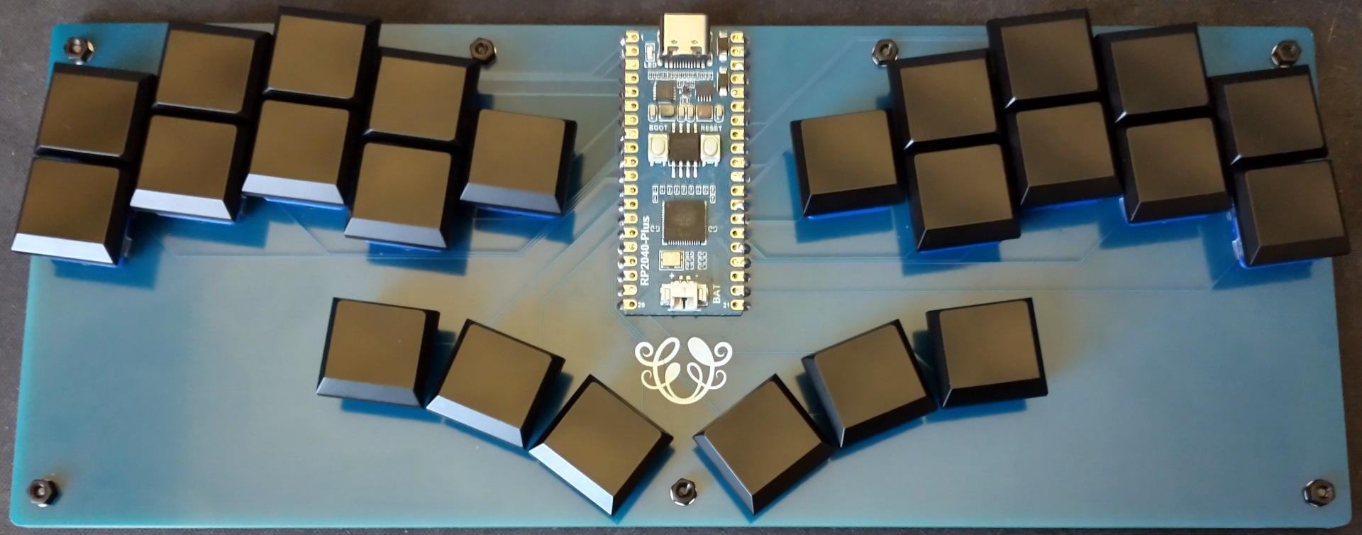
Umbra is a 24 key ergonomic keyboard, powered by a Raspberry Pi Pico.
There are enough keys for playing many games with a keyboard. 2D fighting games like Street Fighter was my personal intent for this build.
The board is a simple rectangle for increased sturdiness, which helps when placing the keyboard on your lap.
gerbers: Gerber files for PCB manufacturinggraphics: Source assets for PCB silkscreenkicad: KiCad project files (schematics and PCB designs)kicad-libraries: KiCad components and footprintsimages: Images for project documentationfirmware: Firmware filesThe PCB is designed for Kailh Choc v1 keyswitches, and supports keycaps designed for 18mm x 17mm spacing.
The Pi Pico footprint uses surface-mount solder pads. The castellated pads of the Pi Pico are used to solder it directly to the PCB.
The keyswitches are directly connected to the GPIO pins of the Pi Pico.
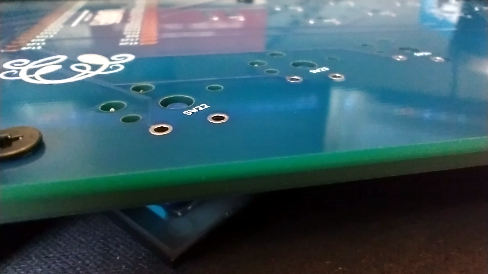
Each build uses two copies of the same PCB. This PCB acts as both the logical PCB, and when flipped the long way, it acts as a bottom plate to be attached the logical PCB.
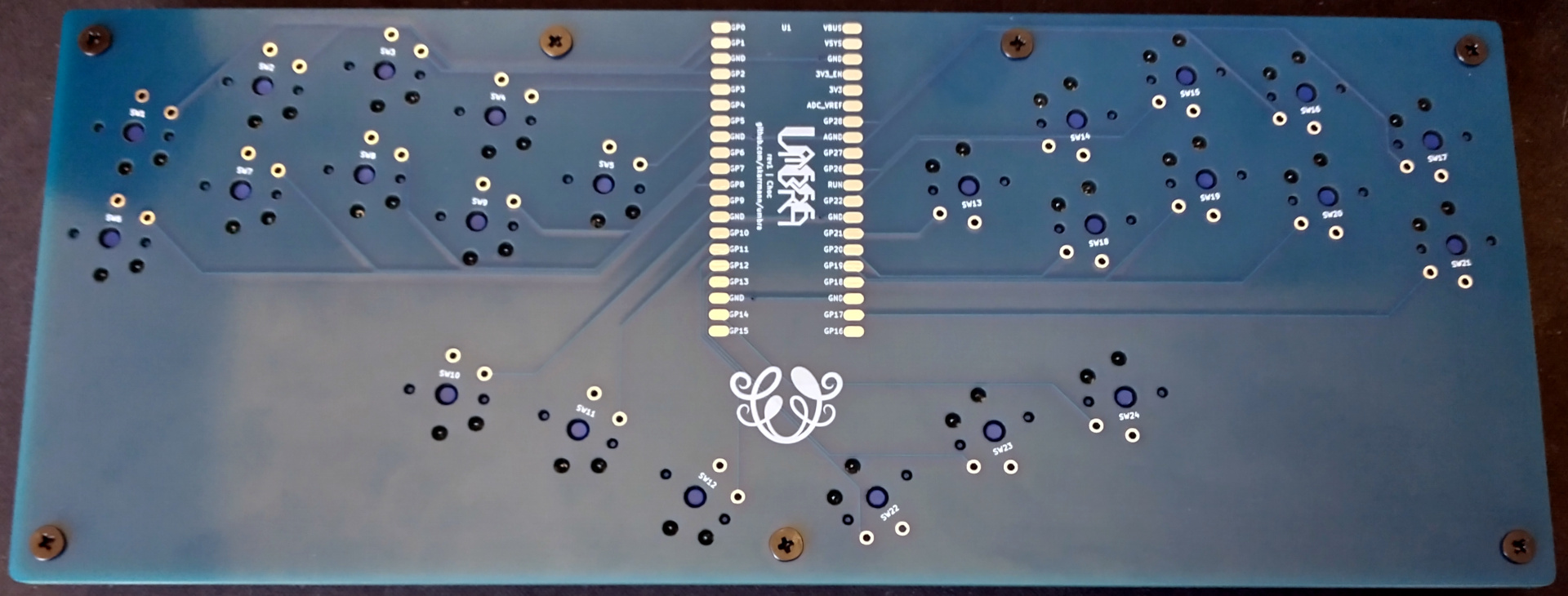
firmware/kmkfirmware/gp2040-ce| Part | Purpose | Quantity | Notes |
|---|---|---|---|
| PCB | circuit board and bottom plate | 2 | Send Gerber zip files to JLCPCB. |
| Raspberry Pi Pico | Microcontroller board | 1 | Supports other boards with the Pico footprint and castellated solder pads (Waveshare RP2040 Plus) |
| Keyswitches | 24 | Kailh Choc V1 keyswitches | |
| Keycaps | 24 | Kailh Choc V1 keycaps (18mm x 17mm) | |
| M2 6mm screws | Secure main PCB and bottom plate PCB | 7 | |
| M2 nuts | Secure main PCB and bottom plate PCB | 7 | |
| 2mm tall rubber bumpons | Raise board above desk surface and provide skid resitance | 8 |
These are the manufacturing settings I used when ordering from JLCPCB:
IMPORTANT: The PCB has "JLCJLCJLCJLC" silkscreen text on the bottom side of the board. If you want to remove the order number from the boards or you want to print the PCBs with another manufacturer, then I recommend removing this silkscreen text from the .kicad_pcb file, and then regenerate the Gerber files.
The keyswitch footprints have cutouts for their through-hole solder pads, rotated 180 degrees from the center of the footprint. On opposite halves of the PCB, the keyswitch footprints are rotated 180 degrees. This allows the cutouts to encase the solder pads when the PCB is flipped and used as a bottom plate.
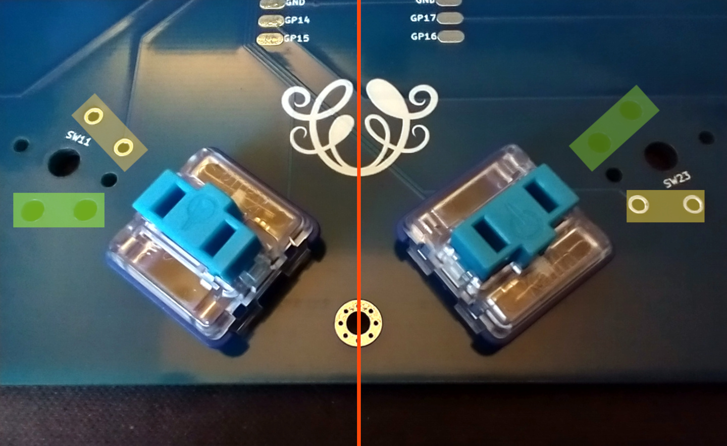
This project contains KiCad footprints for both Choc and MX switches with these mounting cutouts. There are also footprints and symbols for other microcontroller boards with castellated pads considered for the design (Waveshare RP-2040 Zero and Seeed XIAO RP2040).
Here are guidelines for using Umbra's self-encasing PCB construction approach for your own designs:
| Qty | Value | Footprint | References |
|---|---|---|---|
| 24 | SW_Push | umbra-footprints:SW_Choc_Reverse_Cutout | SW1, SW2, SW10, SW11, SW12, SW13, SW14, SW15, SW16, SW17, SW18, SW19, SW20, SW21, SW22, SW23 +8 |
| 7 | Hole_Pad | umbra-footprints:Mount_M2 | H1, H2, H3, H4, H5, H6, H7 |
| 1 | Logo-Graphic | umbra-footprints:Logo_Umbra | LOGO2 |
| 1 | Logo-Name | umbra-footprints:Logo_Umbra_Name | LOGO1 |
| 1 | Pi Pico | umbra-footprints:Pi-Pico_SMD | U1 |
It measures 224 × 89 mm and has 2 copper layers, 1.6 mm thick.
34 parts. The full list of its parts is on this page, with links to each part's symbol and footprint where PCBKit's library has them.
From the skarrmann/umbra repository on GitHub, at the commit this page was made from: the board is kicad/choc/umbra-choc.kicad_pcb and its schematic kicad/choc/umbra-choc.kicad_sch. PCBKit opens the board in the browser, with nothing to install.
Its repository publishes it under the MIT licence: you may reuse it on that licence's terms (keep the author's notice, and for a copyleft licence share your changes alike).

FrameworkComputer/ExpansionCards
Reference designs and documentation to create Expansion Cards for the Framework Laptop

mntmn/amiga2000-gfxcard
MNT VA2000, an Open Source Amiga 2/3/4000 Graphics Card (Zorro II/III), written in Verilog

hackclub/OnBoard
💡 Join 1,000 teenagers and make your first PCB with a $100 grant!


strangeparts/niubi-headphones
Flexible circuit board design for adding a headphone jack to an iPhone 7


baldengineer/bit-preserve
Project for capturing vintage, classic, aka old computer schematics in KiCad.