
2 layers104.9 × 75.2 mm
 sitlesh/ATmega328P-Custom-Development-Board
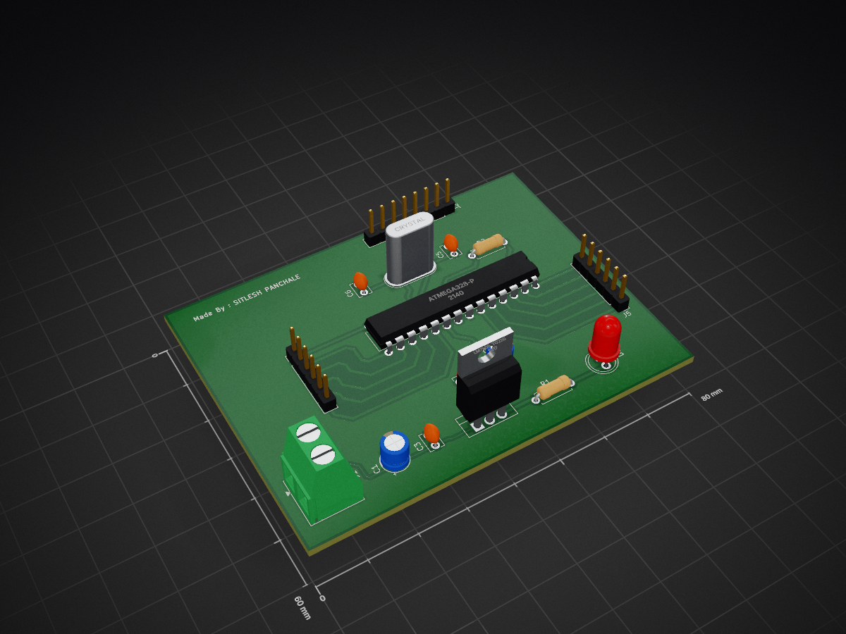
A custom-designed, compact ATmega328P microcontroller board with an on-board 5V voltage regulator
ATmega controller board is an open-source printed circuit board by sitlesh, from the sitlesh/ATmega328P-Custom-Development-Board repository on GitHub. It is a 2-layer board of 80 × 60 mm with 16 parts on 28 nets, routed with 139 tracks and 0 vias.
It is built around the ATMEGA328-PU. Its parts include 6 capacitors, 4 connectors, 2 resistors, 2 ICs and 1 diode. It belongs with the microcontroller boards boards and the AVR (ATmega, ATtiny) boards of this library.
An industry-standard, standalone microcontroller development board designed using KiCad 10.0. This project serves as a robust hardware platform for learning circuit design, power regulation, and microcontroller prototyping.
The board breaks out all digital and analog pins of the ATmega328P microcontroller to standard 2.54mm pin headers while integrating a clean power management section to ensure stable operation.
This repository contains all the native design assets and manufacturing files required to replicate or modify this project.
ATmega controller board.kicad_sch - Schematic capture showing the ATmega328P microcontroller core, LM7805 voltage regulation circuit, decoupling networks, and crystal loading capacitors.ATmega controller board.kicad_pcb - Physical PCB layout featuring optimized signal trace routing, 45° angles, and solid ground planes.ATmega controller board.kicad_pro - KiCad project management file.Gerber.zip - Production-ready manufacturing package containing all necessary layers (Copper, Solder Mask, Silkscreen) and NC Drill files, ready to upload directly to JLCPCB, PCBWay, etc.| Qty | Value | Footprint | References |
|---|---|---|---|
| 2 | 0.1uF | Capacitor_THT:C_Disc_D3.8mm_W2.6mm_P2.50mm | C3, C4 |
| 2 | 10uF | Capacitor_THT:CP_Radial_D5.0mm_P2.00mm | C1, C2 |
| 2 | 22pF | Capacitor_THT:C_Disc_D3.8mm_W2.6mm_P2.50mm | C5, C6 |
| 2 | Conn_01x06_Pin | Connector_PinHeader_2.54mm:PinHeader_1x06_P2.54mm_Vertical | J4, J5 |
| 1 | 10k | Resistor_THT:R_Axial_DIN0207_L6.3mm_D2.5mm_P7.62mm_Horizontal | R2 |
| 1 | 330 | Resistor_THT:R_Axial_DIN0207_L6.3mm_D2.5mm_P7.62mm_Horizontal | R1 |
| 1 | ATmega328-P | Package_DIP:DIP-28_W7.62mm | U2 |
| 1 | Conn_01x08_Pin | Connector_PinHeader_2.54mm:PinHeader_1x08_P2.54mm_Vertical | J2 |
| 1 | Crystal | Crystal:Crystal_HC49-U_Vertical | Y1 |
| 1 | LED | LED_THT:LED_D5.0mm | D1 |
| 1 | LM7805_TO220 | Package_TO_SOT_THT:TO-220-3_Vertical | U1 |
| 1 | Screw_Terminal_01x02 | TerminalBlock_Phoenix:TerminalBlock_Phoenix_MKDS-1,5-2_1x02_P5.00mm_Horizontal | J1 |


peej/lumberjack-keyboard
5x12 ortholinear through-hole component keyboard PCB for standard 60% cases

peterheinrich/InternetOverSpaghetti
Transmitting IP packages over a pair of spaghetti thus demonstrating how media independent IP really is.


It measures 80 × 60 mm and has 2 copper layers, 1.6 mm thick.
16 parts, built around the ATMEGA328-PU. The full list of its parts is on this page, with links to each part's symbol and footprint where PCBKit's library has them.
From the sitlesh/ATmega328P-Custom-Development-Board repository on GitHub, at the commit this page was made from: the board is ATmega controller board.kicad_pcb and its schematic ATmega controller board.kicad_sch. PCBKit opens the board in the browser, with nothing to install.
Its repository states no licence, so its author keeps all rights: ask sitlesh before reusing the design.