


2 layers100 × 70 mm
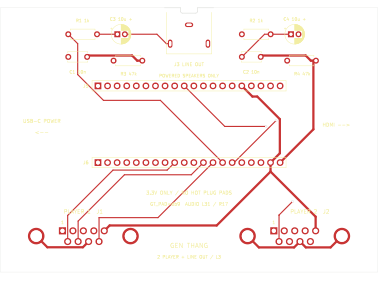
Dual db9-opt pcb unrouted
shawnchivers/genthang
Sega Mega Drive / Genesis core for the Sipeed Tang Nano 20K (alpha)
8 parts6GPL-3.0

 shawnchivers/genthang6
Sega Mega Drive / Genesis core for the Sipeed Tang Nano 20K (alpha)
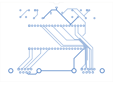
Dual db9-lineout pcb unrouted is an open-source printed circuit board by shawnchivers, from the shawnchivers/genthang repository on GitHub, published under the GPL-3.0 licence. It is a 2-layer board of 100 × 70 mm with 17 parts on 22 nets, routed with 6 tracks and 0 vias.
Its parts include 5 connectors, 4 capacitors and 4 resistors.
Start building: the illustrated L3 assembly guide includes a simple capacitor chooser, soldering steps, pre-power checks and firmware downloads.
O1 plus a stereo 3.5 mm line-out, all through-hole for easy
DIY soldering. Same Nano socket parts, the same two DB9 ports and the same canonical
GT_PAD=db9 pinout as O1, so player wiring and controllers are unchanged. The line-out
works in both HDMI and DVI modes, so a TV that flickers with HDMI data islands can run
in Video output: DVI+LINE OUT and get sound from powered speakers.
L3 keeps L2's Tang orientation on its top-mounted female headers: USB-C power left, HDMI right, audio at the rear, DB9 ports at the front. No separate power connector is added; the existing Tang USB-C port remains the power input.
L3 changes only the right-audio connection: GPIO17 at J6 contact 15 now feeds R2, instead of GPIO56 at J5 contact 7. Both DB9 player pinouts, left audio, filter parts, dimensions and connector locations are unchanged. The Tang plugs directly into L3 with no audio jumper; J5 contact 7 is unconnected on this carrier. GPIO17 is unused by the controller ports but has the Nano's on-board LED2 load (510 Ω to the LED supply). No LED modification is required for the selected pin test; this revision does not guarantee noise-free audio.
Upload dual-db9-lineout-L3-OSHPARK.zip to OSH Park using its standard two-layer, 1 oz, 1.6 mm service. Do not reorder from an L1/L2 ZIP. This package contains only the two copper, two mask, two silkscreen, outline, plated-drill and non-plated-drill files. Confirm the preview shows 100 × 70 mm, two copper layers, the rear jack notch and three 0.60 × 1.40 mm plated jack slots before paying. Check the L3 marking on the silkscreen. The author confirms successful testing of the GPIO17 right-audio move and has submitted L3 to OSH Park. See the test status for the scope of that confirmation; this remains a prototype fabrication package, not a production qualification.
Verify the files with sha256sum -c SHA256SUMS from this directory. The
validation report covers the firmware pin contract,
schematic/PCB equivalence, connector clearance, drill and annular-ring limits,
and DRC. Same board outline and mount/connector positions as L2, so its cases
remain mechanically compatible.
| Ref | Qty | Part | Notes |
|---|---|---|---|
| J5, J6 | 2 | Harwin M20-7822046, 1×20 female socket, 2.54 mm, 8.5 mm tall | any similar 1×20 female header fits |
| J1, J2 | 2 | Kycon K22X-E9P-N, right-angle male DB9 | other DB9 parts are not fit-checked |
| J3 | 1 | CUI / Same Sky SJ1-3523N, 3.5 mm stereo jack, right angle | footprint is for this part |
| R1, R2 | 2 | 1 kΩ, ¼ W axial, 7.62 mm (0.3 in) pitch | |
| R3, R4 | 2 | 47 kΩ, ¼ W axial, 7.62 mm pitch | 22k–100k is fine |
| C1, C2 | 2 | 10 nF (code 103) ceramic disc or film, 5.0 mm pitch | |
| C3, C4 | 2 | 10 µF 16 V+ radial electrolytic, 5 mm dia, 2.0 mm pitch | polarized |
Full list with descriptions: BOM.csv.
Nano pin ──R1/R2 1k──┬──C3/C4 10µF (+ toward R)──┬──► jack tip (L) / ring (R)
                     │                           │
                  C1/C2 10nF                 R3/R4 47k
                     │                           │
GND ─────────────────┴───────────────────────────┴──► jack sleeve| Channel | FPGA pin | Nano contact | Jack |
|---|---|---|---|
| Left | GPIO31 (audio_jack_l) | J6.14 | tip, J3 pin 2 |
| Right | GPIO17 (audio_jack_r) | J6.15 | ring, J3 pin 3 |
| Ground | GND | J6.20 / J5.15 | sleeve, J3 pin 1 |
The 1 kΩ and 10 nF turn GenThang's 1-bit audio into an analog signal (≈16 kHz corner). The 10 µF blocks the 1.65 V DC level. R3/R4 are extra compared with the README breadboard filter: they keep the output side of the capacitor at 0 V so plugging in a speaker does not give a loud pop. Output is about 1 V peak to peak: powered speakers, a soundbar or an amplifier, not headphones.
For a darker, original Genesis Model 1-style frequency response, replace only C1 and C2, one per channel. Keep R1/R2 at 1 kΩ:
| Filter option | C1 and C2 | Capacitor marking | Nominal cutoff |
|---|---|---|---|
| Stock L3 | 10 nF | 103 | 15.9 kHz |
| Model 1 VA0–VA2-style | 47 nF | 473 | 3.39 kHz |
| Model 1 VA3–VA6-style | 56 nF | 563 | 2.84 kHz |
Simple choice: start with two 10 nF (103) capacitors for the stock
response. Choose 47 nF (473) for a darker VA0–VA2-style response, or
56 nF (563) for a darker VA3–VA6-style response.
For the 56 nF option, use two film capacitors, 5% tolerance, 50 V,
5.0 mm lead spacing. These are nonpolarized; either direction works. Check the
chosen capacitor's body dimensions against the board and enclosure before buying.
Use the same value in both channels. Power off and unplug USB before replacing parts.
Leave R3/R4 at 47 kΩ and C3/C4 at 10 µF. The electrolytics remain polarized, with their positive leads toward R1/R2, not the jack. No PCB trace or firmware changes are required. The BOM, schematic and fabrication files retain the stock 10 nF value; these substitutions are optional assembly variants.
The nominal corners use fc = 1 / (2 * pi * R * C). R3/R4 and the connected
amplifier input load the filter, shifting the actual corner and output level; use a
high-impedance line input. These values approximate the analog low-pass cutoff,
not the complete sound of an original console's DAC, mixer and amplifier, or any
filtering already applied in firmware. This optional response has not been
hardware-measured on L3.
The revision-specific targets (3.39 kHz for VA0–VA2 and 2.84 kHz for VA3–VA6) are described in Genesis & Sega CD - Audio Filtering. This recommendation does not cover the different Model 1 VA7 audio circuit.
Unchanged from O1; see its connection table. Player 1 is entirely on J6 and player 2 entirely on J5. Pin 5 of each DB9 is 3.3 V.
Use a DB9 build with audio_jack_l on GPIO31 and audio_jack_r on GPIO17.
This is already on GenThang main.
Download the packaged GPIO17 flash image
and its checksums.
Released images through 1.9.2 output right audio on GPIO56 and do not match L3.
The generator reads the pin assignments, including the two audio pins, from
genthang/src/boards/nano20k_db9.cst; a copy is in
reference/built-pinout.cst, and the check fails if the
board, schematic and constraints disagree.
When this design is imported under GenThang's hardware/ directory, the generator
reads that repository's src/boards/nano20k_db9.cst directly.
L1/L2 compatibility: with the Tang removed from the carrier, an isolated jumper from Tang J6.15 to PCB J5.7 can feed the old right filter from the new firmware. Do not also connect Tang J5.7 (GPIO56) to that filter. Power off before rewiring.
KiCad DRC: 0 violations, 0 unconnected pads. The firmware pin contract, the line-out circuit contract and schematic/PCB equivalence pass. The author has confirmed that moving right audio to GPIO17 works and has submitted L3 to OSH Park. See TEST-STATUS.md for the distinction between this bench confirmation and the generated CAD report. Slot width, drill size, annular rings, and module/cable corridor placement are checked explicitly in addition to DRC. L3 supersedes the L1/L2 fabrication ZIPs for GPIO17 firmware. Same limits as O1: no ESD protection or buffering, 3.3 V pads only, no controller hot plug. Keep the Nano's speaker and LCD connectors empty.
Via bash ../cad-python: build_board.py generate, route (Freerouting), import
(also runs the checks and native DRC), export. Regression tests:
bash ../cad-python -m unittest discover -s . -p 'test_build_board.py'.
After documentation-only edits, refresh the release manifest without recreating
the already-ordered Gerbers:
bash ../cad-python build_board.py checksums. The manifest includes the illustrated
guide, its SVG assets and the test-status note.
| Qty | Value | Footprint | References |
|---|---|---|---|
| 4 | M2.5_clearance | DualDB9LineOut:Mount_M2_5 | H1, H2, H3, H4 |
| 2 | 10nF | DualDB9LineOut:C_Disc_D5.0mm_W2.5mm_P5.00mm | C1, C2 |
| 2 | 10uF | DualDB9LineOut:CP_Radial_D5.0mm_P2.00mm | C3, C4 |
| 2 | 1k | DualDB9LineOut:R_Axial_DIN0207_L6.3mm_D2.5mm_P7.62mm_Horizontal | R1, R2 |
| 2 | 47k | DualDB9LineOut:R_Axial_DIN0207_L6.3mm_D2.5mm_P7.62mm_Horizontal | R3, R4 |
| 2 | Nano_socket_1x20 | DualDB9LineOut:Harwin_M20-7822046_1x20 | J5, J6 |
| 1 | GENESIS_3V3_PLAYER1 | DualDB9LineOut:Kycon_K22X-E9P-N | J1 |
| 1 | GENESIS_3V3_PLAYER2 | DualDB9LineOut:Kycon_K22X-E9P-N | J2 |
| 1 | LINE_OUT_3.5mm | DualDB9LineOut:Jack_3.5mm_CUI_SJ1-3523N_Horizontal | J3 |
shawnchivers/genthang
Sega Mega Drive / Genesis core for the Sipeed Tang Nano 20K (alpha)


hoglet67/RGBtoHDMI
Bare-metal Raspberry Pi project that provides pixel-perfect sampling of Retro Computer RGB/YUV video and conversion to HDMI


hackclub/OnBoard
💡 Join 1,000 teenagers and make your first PCB with a $100 grant!

DDeGonge/OS-ARM
This arm is not industrial and it will not be fast, but that is not my goal. But it will hopefully be a very nice looking arm fully capable of 6dof motion, cheap enough to keep it accessable but capable enough to…


It measures 100 × 70 mm and has 2 copper layers, 1.6 mm thick.
17 parts. The full list of its parts is on this page, with links to each part's symbol and footprint where PCBKit's library has them.
From the shawnchivers/genthang repository on GitHub, at the commit this page was made from: the board is hardware/dual-db9-lineout-pcb/dual-db9-lineout-pcb-unrouted.kicad_pcb and its schematic hardware/dual-db9-lineout-pcb/dual-db9-lineout-pcb.kicad_sch. PCBKit opens the board in the browser, with nothing to install.
Its repository publishes it under the GPL-3.0 licence: you may reuse it on that licence's terms (keep the author's notice, and for a copyleft licence share your changes alike).