


2 layers85.1 × 53.3 mm
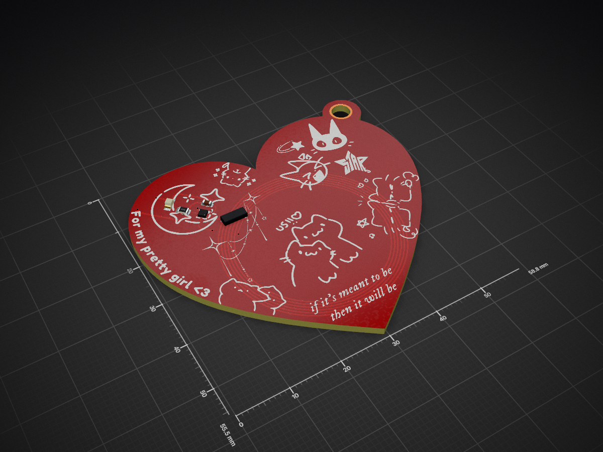
A heart shaped NFC Card with cute silkscreen art and a keyring!
Eva is an open-source printed circuit board by Shadow220108, from the Shadow220108/Eva repository on GitHub. It is a 2-layer board of 58.8 × 55.5 mm with 26 parts on 8 nets, routed with 70 tracks and 6 vias.
It is built around the NT3H2111W0FHKH and KT-0805G. Its parts include 1 capacitor, 1 resistor, 1 IC and 1 diode. It belongs with the radio and wireless boards of this library.
A heart shaped NFC Hacker Card!
The PCB is 2 layers with dimensions under 100 by 100mm, it is designed to be in a heart shape has some cool silkscreen with black color cause black colored PCBs are cool.
Here are the schematics
| Schematics |
|---|
It was made for Expedition Ireland! And to give as a gift for my friends :D
| Component | Qty | Price | Vendor |
|---|---|---|---|
| PCB | 5 ( MOQ ) | 2$ | JLCPCB |
| PCBA | 2 ( MOQ ) | 17.16$ | JLCPCB |
| Shipping | 8.93$ | ||
| Total | 28.09$ |
| Qty | Value | Footprint | References |
|---|---|---|---|
| 16 | LOGO | LOGO | G***, G***, G***, G***, G***, G***, G***, G***, G***, G***, G***, G***, G***, G***, G***, G*** |
| 4 | TestPoint_Probe | TestPoint:TestPoint_Pad_1.5x1.5mm | SCL, TP1, VCC, VSS |
| 1 | 17-21SUYC/TR8 | easyeda2kicad:LED0805-R-RD | LED1 |
| 1 | 220nF | Capacitor_SMD:C_0603_1608Metric | C1 |
| 1 | 47R | Resistor_SMD:R_0805_2012Metric | R1 |
| 1 | Antenna_Loop | easyeda2kicad:NFC_36x36_N6_NXP_PN5180 | AE1 |
| 1 | NT3H2111W0FHKH | easyeda2kicad:XQFN-8_L1.6-W1.6-P0.50-BL_NT3H2111W0FHKH | U1 |
The 25 most common of 26 parts.
It measures 58.8 × 55.5 mm and has 2 copper layers, 1.6 mm thick.
26 parts, built around the NT3H2111W0FHKH and KT-0805G. The full list of its parts is on this page, with links to each part's symbol and footprint where PCBKit's library has them.
From the Shadow220108/Eva repository on GitHub, at the commit this page was made from: the board is PCB/eva.kicad_pcb and its schematic PCB/eva.kicad_sch. PCBKit opens the board in the browser, with nothing to install.
Its repository states no licence, so its author keeps all rights: ask Shadow220108 before reusing the design.

darshg321/fallout-badge
its a little whale-shaped PCB with NFC! it has an LED for the eye.


nushackers/hnr26-badge-quacknroll
Hack&Roll 2026 "Quack & Roll" badge source files, for both hardware and firmware


ElectronicCats/badge-dragonJar-2025
¡El badge oficial de DragonJarCON 2025! Un dispositivo NFC programable con pantalla OLED, múltiples LEDs y un reto de hacking integrado. Diseñado para la comunidad de DragonJar