2 layers
Encoder
byrantech/laptop
anyon_e, a highly integrated, high end, open source laptop. Attempt the impossible.
7 parts4.3kMIT

 seanysebo-2/ESP32-IR-Remote-Decoder
ESP32 infrared remote controller with custom PCB design in KiCad, IR signal decoding, storage, and transmission.
Esp32 project is an open-source printed circuit board by seanysebo-2, from the seanysebo-2/ESP32-IR-Remote-Decoder repository on GitHub. It is a 2-layer board of 64.5 × 96.5 mm with 7 parts on 30 nets, routed with 50 tracks and 0 vias.
Its parts include 4 switches and 3 connectors. It belongs with the ESP32 boards of this library.
This project focuses on developing an ESP32-based infrared remote controller capable of receiving, decoding, storing, and transmitting infrared signals.
I initially developed and tested the circuit using a breadboard before transitioning to a custom PCB design using KiCad.
The goal of this project is to gain hands-on experience with electronics, microcontrollers, PCB layout, and hardware development.
Developed a working ESP32-based circuit capable of receiving and decoding infrared signals using the Arduino IRremote library.
Implemented functionality for storing received infrared commands and transmitting them through an infrared LED.
Designed a custom PCB using KiCad to transition the project from a breadboard prototype to a more permanent hardware platform.
The PCB design includes:
The PCB design has been prepared for manufacturing. The next stage involves assembling the physical components and testing the completed board.
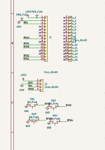
The schematic shows the ESP32 GPIO connections, infrared receiver and transmitter connections, and four tactile push buttons.
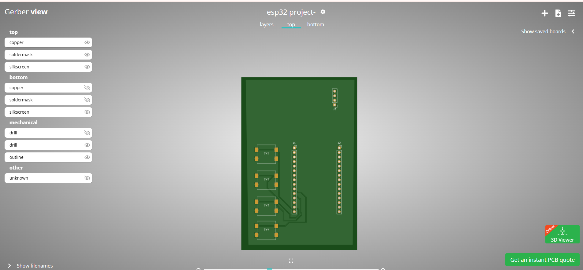
The PCB was designed in KiCad using front and back copper layers, component placement, copper trace routing, and ground planes.
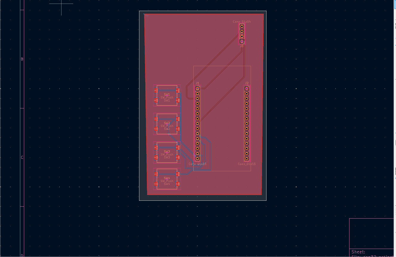
The 3D model shows the physical PCB design and component placement.
| Qty | Value | Footprint | References |
|---|---|---|---|
| 4 | SW_Push | IR_Remote:SW_Tactile_SMD_10x10mm | SW1, SW2, SW3, SW4 |
| 2 | Conn_01x15 | Connector_PinSocket_2.54mm:PinSocket_1x15_P2.54mm_Vertical | J1, J2 |
| 1 | Conn_01x04 | Connector_PinHeader_2.54mm:PinHeader_1x04_P2.54mm_Vertical | J3 |
byrantech/laptop
anyon_e, a highly integrated, high end, open source laptop. Attempt the impossible.


AxxAxx/AxxSolder
STM32 Based soldering station for JBC cartridges, 9-24 VDC and USB-PD power


jamro/tiny-engineer
A small desktop robot that brings an AI coding assistant to life, physically acting out when it reads files, thinks, writes code, and finishes work.

hoglet67/RGBtoHDMI
Bare-metal Raspberry Pi project that provides pixel-perfect sampling of Retro Computer RGB/YUV video and conversion to HDMI

It measures 64.5 × 96.5 mm and has 2 copper layers, 1.6 mm thick.
7 parts. The full list of its parts is on this page, with links to each part's symbol and footprint where PCBKit's library has them.
From the seanysebo-2/ESP32-IR-Remote-Decoder repository on GitHub, at the commit this page was made from: the board is esp32 project.kicad_pcb and its schematic esp32 project.kicad_sch. PCBKit opens the board in the browser, with nothing to install.
Its repository states no licence, so its author keeps all rights: ask seanysebo-2 before reusing the design.