

2 layers83.3 × 65.3 mm
SimonShield
github-linguist/linguist
Language Savant. If your repository's language is being reported incorrectly, send us a pull request!
46 parts14kMIT
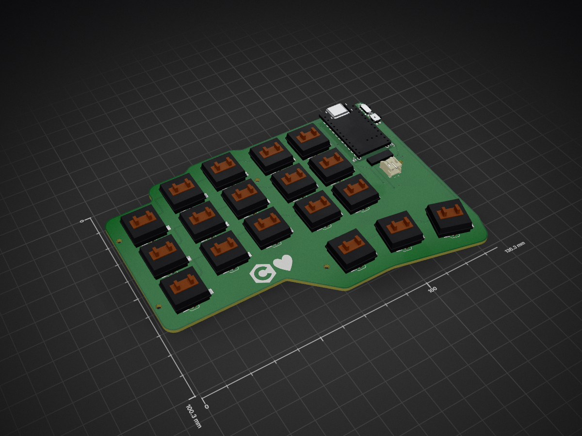
 schultz-dev0/cloudy-36-kb
This repo contains a complete design for a 36 key split wireless keyboard. Fabricate two copies and flip one for the opposite half.
Cloudy-36-kb is an open-source printed circuit board by schultz-dev0, from the schultz-dev0/cloudy-36-kb repository on GitHub. It is a 2-layer board of 136.3 × 100.2 mm with 46 parts on 68 nets, routed with 818 tracks and 110 vias.
Its parts include 18 diodes and 18 switches. It belongs with the keyboards and input boards of this library.
This repo contains a complete design for a 36 key split wireless keyboard. Fabricate two copies and flip one for the opposite half.
The board uses Kailh Choc hot swap sockets (Choc v2 switches) and one nice!nano v2 and nice!view per half, each half also contains one 110 mAh 301230 LiPo battery.
Board has 5 M2 mounting holes per half. A 3D-printed case (tray + top deck that doubles as the switch plate) is in cad/; the case uses 4 of the holes. Keycaps are low-profile MX-stem.
Populate all visible components on the top face of each assembled half: use the front side of one PCB and the back side of the other. Choc sockets and diodes go on the underside. Bridge only the jumper pads for the chosen nice!nano, nice!view, and JST side. The YAML disables footprint-supplied copper links, so those short jumper connections are part of the manual routing work too.
Full list in bom.csv.
| Category | Item | Qty | On pre-soldered board | Notes |
|---|---|---|---|---|
| PCB | Custom PCB (reversible) | 2 | n/a | order gerbers from reversible.kicad_pcb, flip one when populating |
| Switches | Key switches | 36 (18/half) | No | Kailh Choc v2 (PG1353) low-profile, e.g. salvaged Lofree Flow Lite switches; hot-swap, you press these in yourself; PCB centre hole is 5.0 mm for the v2 post |
| Switches | Hot-swap sockets | 36 (18/half) | No | Kailh Choc hot-swap socket, 1 per switch; the footprint itself is flagged excluded from assembly by ceoloide, always hand-soldered |
| Switches | Keycaps | 36 (18/half) | No | low-profile MX-stem keycaps (Choc v2 cross stem), e.g. salvaged Lofree caps; layout assumes 17.5x16.5mm keycaps |
| Switches | Diodes | 36 (18/half) | Yes | 1N4148W, SOD-123 package |
| Controller | nice!nano v2 | 2 (1/half) | No | controller module; socketed not soldered directly, plug in after flashing ZMK |
| Controller | nice!nano socket headers | 4 (2/half) | No | medium-profile sockets, 2 rows of 12 + 25 pins per controller; case CAD assumes ~3.8 mm nano standoff (nano_socket_height); measure and update |
| Controller | nice!view display | 2 (1/half) | No | display module; socketed like the nano |
| Controller | nice!view socket headers | 2 (1/half) | No | 5-pin socket + header, bundled with the display; case CAD assumes ~8.3 mm PCB-to-display (display_socket_height); must clear the nano USB-C shell |
| Power | LiPo battery | 2 (1/half) | No | 110mAh 301230, protected, JST PH 2.0 connector; sits under the PCB between the nano socket rows; leads go up through the old 3.5 mm trackpoint hole to the JST; check polarity |
| Power | Battery connector | 2 (1/half) | Yes | JST PH 2-pin |
| Power | Power switch | 2 (1/half) | Yes | side-actuated SMD slide switch |
| Power | Reset switch | 2 (1/half) | Yes | side-actuated SMD switch |
| Case | Case tray | 2 (1/half) | n/a | 3D-printed, white; floor, walls, USB-C / power / reset openings, MagSafe recess |
| Case | Top deck | 2 (1/half) | n/a | 3D-printed, white, 1.2 mm; doubles as the switch plate (plate.dxf cutouts); open window over the nano, nice!view and power/reset; C♥ logo inlay |
| Case | Plate foam | 2 (1/half) | n/a | thin foam (Poron-like) between PCB and deck, cut to plate.dxf; e.g. salvaged Lofree plate foam |
| Case | Bottom foam | 2 (1/half) | n/a | spongy foam bed under the PCB, ~3.5 mm, pocketed for the battery; e.g. salvaged Lofree case foam |
| Case | MagSafe sticker | 2 (1/half) | n/a | MagSafe-compatible steel ring sticker; sits in the floor recess, sticks to tenting stands and clamps |
| Case | M2 screws | 8 (4/half) | n/a | M2 x 6 countersunk; through the deck and PCB mounting holes MH1-MH4 |
| Case | Heat-set inserts | 8 (4/half) | n/a | M2 brass heat-set insert, ~3.2 mm OD x 3 mm; melted into the tray posts |
The matrix is column-to-row through one 1N4148W diode per key. The nice!view uses P1 for CS, P2 for MOSI, and P3 for SCK. Each protected LiPo connects to its JST header; battery positive passes through the power switch to RAW, while battery negative connects to GND. Leave the nice!nano charge-rate boost jumper open for a 110 mAh battery.
Always verify battery connector polarity against the actual battery before plugging it in. Confirm part availability and assembly rotation in the board house preview before placing an order.
The third-party footprint sources in footprints/ retain their upstream
license headers. Project-specific keepout footprints are kept alongside them.
Open output/cad/cloudy-choc-36.FCStd in
FreeCAD, or import output/cad/cloudy-choc-36.step
into another CAD application. Separate left-half.step and right-half.step
exports are in the same directory. The FreeCAD tree groups individually
selectable BOM components under each half, with named housing, contact, and
other subfeatures. These are editable solid models, not a constrained mechanical
assembly or manufacturing models for the purchased parts.
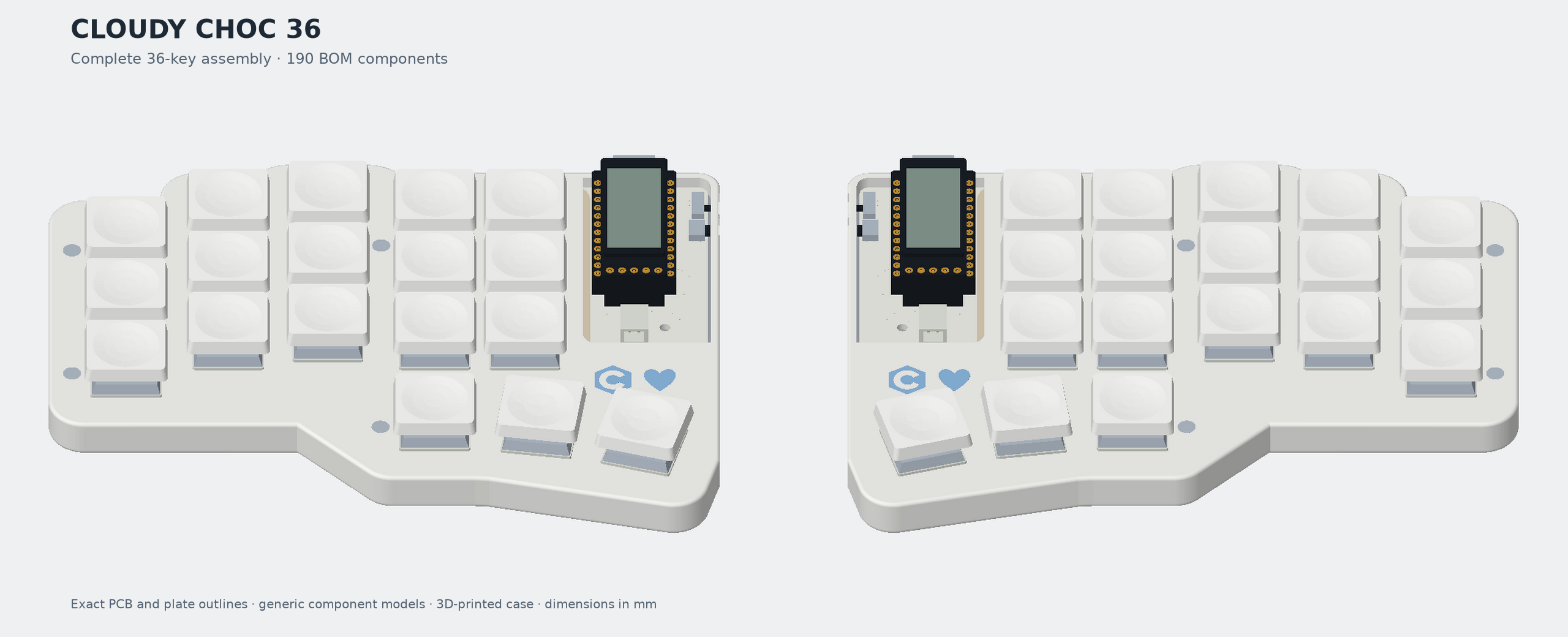
Exploded left half · Underside · Instantiated BOM · Geometry validation
The generator reads bom.csv and checks all 179 component instances against it.
PCB edge curves, thickness, footprint positions, rotations, and pad/via drills
come from the current reversible.kicad_pcb. The right PCB is flipped with its
back populated; switches and sockets retain their manufactured handedness.
The original plate.dxf supplies the plate geometry, including 18 switch
openings and four mounting holes per half. The fifth PCB mounting hole is in
the electronics area outside the plate. Sockets and diodes are placed underneath,
following the assembly instructions above rather than the fabrication CSV's
layer field.
CAD assumptions are editable in cad/parameters.json:
| Detail | Model choice |
|---|---|
| Layout | Both halves flat, 32 mm apart; left is the central TrackPoint half |
| PCB | 1.6 mm from KiCad; drilled substrate, without copper traces or silkscreen |
| Plates | 1.2 mm thick; upper surface 2.2 mm above the PCB top |
| Switches | Generic Choc V1: 15 mm housing rim, 5 mm housing height, 3 mm exposed stem; twin slots and locating/contact pins |
| Caps | Blank, tapered, dished, hollow 17.5 × 16.5 mm caps with twin Choc prongs; 3 mm shell height; shell bottom 7.5 mm above PCB |
| Controller | 17.78 × 33.08 mm footprint envelope; generic radio package and USB-C shell; 1 mm module PCB |
| Sockets | 5 mm controller sockets; 10 mm display socket; 2.54 mm pitch at the actual footprint holes |
| Display | 14 × 36 mm config envelope; generic bezel and reflective screen; 1 mm module PCB |
| Battery | Nominal 3 × 12 × 30 mm pouch, 0.2 mm above PCB, beneath controller |
| TrackPoint | Generic T460s-style bracket/sensing head at TP1, using the footprint's 19.5 mm bracket-hole spacing and configured 3.5 mm stick hole; cap at key height |
| Resistors | Both optional 0805 pull-ups shown fitted on the central half |
| Screws | Ten generic M2 × 6 mm envelopes with hex recesses; threads omitted |
The generic switch dimensions use the manufacturer's PG1350 drawing. The local footprint outlines supply the controller, connector, controls, and TrackPoint reference geometry. Unspecified socket heights, keycap profile, component details, and screw lengths are assumptions for this assembly. Battery wires and the salvaged TrackPoint's remote controller/flex are not dimensioned in the repo and are not modeled. No case, spacers, or nuts are specified in the BOM. Confirm these choices against the actual purchased parts before designing a case.
To rebuild, use Python with the FreeCAD Python modules and PyYAML installed
(the script also checks /usr/lib/freecad/lib on Linux):
python cad/build.py
python cad/present.py --gui
python cad/verify.py
The second command needs NumPy, Matplotlib, and a working Qt GUI environment. It
stores colors and the initial camera, exports colored STEP files, and renders
previews directly from the CAD solids. Prefix it with QT_QPA_PLATFORM=offscreen
for a display-independent run. Omit --gui to render only the previews. The
third command independently reopens the native file and all three STEP exports,
checking visibility, BOM counts, solid validity, solid counts, volumes, dimensions,
and STEP colors; its results are added to the validation report.
Edit the JSON parameters and rebuild to change the stack; the document's build
parameter properties record the settings and do not drive live recomputation.
The validation report records BOM counts, solid validity, component intersection
volumes above 0.01 mm³, and source hashes. It is a nominal mechanical check, not
an electrical, tolerance, switch-travel, or manufacturing validation.
| Qty | Value | Footprint | References |
|---|---|---|---|
| 18 | ceoloide:switch_choc_v1_v2 | S1, S2, S3, S4, S5, S6, S7, S10, S11, S12, S13, S14, S15, S16, S17, S18 +2 | |
| 18 | ceoloide:diode_tht_sod123 | D1, D2, D3, D4, D5, D6, D7, D10, D11, D12, D13, D14, D15, D16, D17, D18 +2 | |
| 5 | ceoloide:mounting_hole_npth | MH1, MH2, MH3, MH4, MH5 | |
| 1 | ceoloide:display_nice_view | DISP1 | |
| 1 | ceoloide:reset_switch_smd_side | RST1 | |
| 1 | ceoloide:battery_connector_jst_ph_2 | JST1 | |
| 1 | ceoloide:power_switch_smd_side | PWR1 | |
| 1 | ceoloide:mcu_nice_nano | MCU1 |
It measures 136.3 × 100.2 mm and has 2 copper layers, 1.6 mm thick.
46 parts. The full list of its parts is on this page, with links to each part's symbol and footprint where PCBKit's library has them.
From the schultz-dev0/cloudy-36-kb repository on GitHub, at the commit this page was made from: the board is output/pcbs/reversible.kicad_pcb. PCBKit opens the board in the browser, with nothing to install.
Its repository states no licence, so its author keeps all rights: ask schultz-dev0 before reusing the design.
github-linguist/linguist
Language Savant. If your repository's language is being reported incorrectly, send us a pull request!

byrantech/laptop
anyon_e, a highly integrated, high end, open source laptop. Attempt the impossible.

VoronDesign/Voron-Hardware
Cool Hardware designed by the Voron Design group


hackclub/OnBoard
💡 Join 1,000 teenagers and make your first PCB with a $100 grant!


OLIMEX/DIY-LAPTOP
Do It Yourself Open Source Hardware and Software Modular Hacker's Friendly Laptop