2 layers37 × 19 mm
Passive rpi hub75-adapter
hzeller/rpi-rgb-led-matrix
Controlling up to three chains of 64x64, 32x32, 16x32 or similar RGB LED displays using Raspberry Pi GPIO
2 parts4.4kGPL-2.0

 roffe/ardubdm
Arduino based CPU32 BDM dongle
Ardubdm is an open-source printed circuit board by roffe, from the roffe/ardubdm repository on GitHub. It is a 2-layer board of 57.7 × 22.5 mm with 2 parts on 29 nets, routed with 43 tracks and 0 vias.
It belongs with the AVR (ATmega, ATtiny) boards of this library.
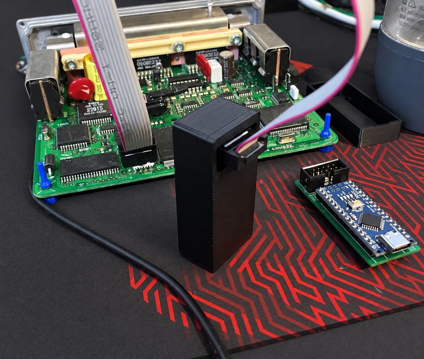
CPU32 (MC68331/MC68332/MC68376/MC68F375, Trionic 5/7/8 ECU) background debug mode adapter on an ATmega328P/PB. Bit-banged BDM, driven over the serial port.
Build with make (make clean to start over; both wrap PlatformIO), flash
with pio run -t upload, or take ardubdm-*.hex
from a GitHub release (tag v*) or the rolling nightly pre-release (rebuilt on every
push to master) and flash it with
avrdude: avrdude -c arduino -p m328pb -P /dev/ttyUSB0 -b 115200 -U flash:w:ardubdm-vX.hex.
10-pin CPU32 BDM header to Arduino pin. All signals sit on PORTD so one register write clocks a bit. Target is 5V CPU32, no level shifting needed.
| BDM pin | Signal | Arduino | AVR | Direction |
|---|---|---|---|---|
| 1 | DS | D8 | PB0 | in, unused by CPU32 BDM, wired for other targets |
| 2 | BERR | D6 | PD6 | input by default; a5/a6/a7 drive low / high / release. Wired to the MCU on the T7 |
| 3 | GND | GND | ||
| 4 | BKPT/DSCLK | D5 | PD5 | out, serial clock while in BDM |
| 5 | GND | GND | ||
| 6 | FREEZE | D4 | PD4 | in, high = target is in BDM |
| 7 | RESET | D7 | PD7 | out low or released, never driven high |
| 8 | IFETCH/DSI | D3 | PD3 | out, data to target (only driven while clocking) |
| 9 | VDD | A0 | PC0 | analog in, target voltage shown by as, not tied to Nano 5V |
| 10 | IPIPE/DSO | D2 | PD2 | in, data from target |
BDM header (top view, pin 1 marked on the ECU board):
 1 DS      2 BERR
 3 GND     4 BKPT/DSCLK
 5 GND     6 FREEZE
 7 RESET   8 DSI
 9 VDD    10 DSO
Connecting the cable to an ECU: the T7 carries the full standard 2x5 header,
so the plug goes on 1:1 with the red stripe at pin 1. The T5 has a 2x4 header
without pins 1 (DS) and 2 (BERR): plug holes 1 and 2, the column at the red
stripe, stay empty and holes 3-10 go on the pins. The two ECUs are rotated
relative to each other. bdmtool's README, "Connecting", has the details. On
the T7, BERR is wired to the MCU: the adapter leaves it as an input
(bdm_init), and a5 really asserts a bus error on the target. The T5 has
no BERR on the header, so a5-a7 do nothing there; a bus cycle stuck
waiting for DSACK is only ended by the CPU's internal bus monitor (bdmtool's
prep turns it on) or by cs.
Pin assignment lives in src/bdm.h. Keep the six BDM signals on the same port if you move them.
All ten header pins are wired so the board can serve other BDM flavours later.
The order was picked so the PCB routes to the header without crossings.
kicad/ holds a KiCad 10 project hat with a shrouded 2x05 IDC box
header for the BDM cable. No other components: the target supplies the
pull-ups on RESET/BKPT/BERR and everything runs at V.
Board: 58 x 22.5 mm, two layers, 0.4 mm tracks. The header stands with its pin rows vertical: with the USB connector on the left, pin 1 is the top-left pin (marked with a triangle) and the shroud key faces the Nano. Signals run on the back and wrap over the top of the header to its outer pin column, RESET and VDD enter the inner column directly, DS and GND run on the front. The Nano's USB end overhangs the left edge.
Serial: 1000000 baud 8N1 (BAUD in src/main.cpp).
0x0d). LF is ignored.0x0d = OK, 0x07 = error.addr8 = 8 digits, v2/v4/v8 = 2/4/8 digits, n2 = 2 digits.c, m or r command fails (block transfers excepted) one err
line precedes the 0x07 flag. FREEZE low: err no target power, VDD x.xxV
(VDD below VDD_MIN_MV, 4.0 V), else err target in reset (RESET low), else
err not in BDM. FREEZE high: the failing frame's response, named
err bus error (10001), err not ready (10000, timed out) or
err illegal command (1FFFF), otherwise err last response xxxxx.a adapter| Command | Action | Reply |
|---|---|---|
av | firmware version | 0103 |
as | pin status and transfer statistics | VDD 4.98V, FREEZE x, RESET x, BKPT x, DSO x, GAP n, RETRIES n, DUMPUS n |
ad | clock one NOP frame, print its raw 17-bit response (diagnostics) | xxxxx |
a1 | drive BKPT low | |
a2 | drive BKPT high | |
a3 | drive RESET low | |
a4 | release RESET (hi-Z) | |
a5 | drive BERR low | |
a6 | drive BERR high | |
a7 | BERR as input |
c target control| Command | Action |
|---|---|
cS | stop: pull BKPT low, wait up to 10 ms for FREEZE |
cR | reset and run: pulse RESET with BKPT released |
cs | restart into BDM: pulse RESET with BKPT held low, wait up to 500 ms for FREEZE |
cb | step: GO then immediately BKPT |
cr<addr8> | run from address. cr00000000 runs from current PC |
cw<addr8>[<ms4>] | run from address and wait for the target to re-enter BDM (a BGND instruction), 2 s or ms4 milliseconds, then print D0. FREEZE must hold for 200 us to count. Used to run code uploaded to target RAM |
m memory (target must be in BDM)| Command | Action | Reply |
|---|---|---|
mb<addr8> | read byte | v2 |
mw<addr8> | read word | v4 |
ml<addr8> | read long | v8 |
mz | dump next byte (address auto-increments from last read) | v2 |
mx | dump next word | v4 |
mc | dump next long | v8 |
mB<addr8><v2> | write byte | |
mW<addr8><v4> | write word | |
mL<addr8><v8> | write long | |
mf<v2> | fill next byte (address auto-increments from last write) | |
mF<v4> | fill next word | |
mM<v8> | fill next long | |
mS<addr8><len4> + data | block write: after the CR send len raw bytes, one flag byte comes back at the end | |
mD<addr8><len4> | block dump: exactly len raw bytes, then the flag byte | len bytes |
Block dump streams straight from BDM, any len up to ffff works. Block
write is limited to len <= 1024 (0400), the serial receive buffer size, because
at 1 Mbaud bytes arrive faster than BDM can write them; a larger block is
drained and refused with 0x07. Accesses are long words where the address
allows, so 4-aligned start addresses are fastest. If BDM fails mid-transfer the
byte count is still honoured (dump pads with zeros, write drains the input) and
the final flag is 0x07. A block write gives up with 0x07 if the host stops
sending for 1 s.
Word and long accesses must be even-aligned.
r registers (target must be in BDM)| Command | Action | Reply |
|---|---|---|
rr<n2> | read system register | v8 |
rW<n2><v8> | write system register | |
ra<n2> | read D/A register | v8 |
rA<n2><v8> | write D/A register | |
rd | display all registers | multi-line dump |
System register numbers:
| n | Register | n | Register |
|---|---|---|---|
| 00 | RPC (return PC) | 0a | VBR |
| 01 | PCC (current instruction PC) | 0b | SR |
| 08 | ATEMP | 0c | USP |
| 09 | FAR (fault address) | 0d | SSP |
| 0e | SFC | ||
| 0f | DFC |
D/A register numbers: 00..07 = D0..D7, 08..0f = A0..A7.
Bench-verified on a Trionic 7 (2026-09-13): reset into BDM, NOP response
0FFFF, full register display, and a full 512 KB block dump (mD) that is
byte-identical to a CombiAdapter read of the same ECU. Full 512 KB dump takes
7 s (pipelined DUMP, assembly bit loop, 1 Mbaud; 2 Mbaud tried, the USB bridge
loses data). Chip erase, block write (mS) and the RAM flash driver (cw +
driver/am29prog.s) verified: a full erase, write and verify of the 512 KB
image takes 25 s with bdmtool, 33 s with a verify dump (the word-by-word
path took 5 minutes).
On a Trionic 5.5 with two AMD 28F010 chips (2026-09-13):
read, chip ID, and the 28F010 RAM driver (driver/am28prog.s) verified: erase,
write and verify of the 256 KB image takes 33 s with bdmtool, with the ECU fed
15V. Not yet verified: the PCB.
tools/bdmcmd.py (pyserial) sends commands from the shell or a prompt and
decodes the replies, including hex dumps for mD and files for mS:
tools/bdmcmd.py -p /dev/ttyUSB5 cs rd ml00040000
tools/bdmcmd.py -p /dev/ttyUSB5 # interactivecs -> 0x0d (target reset into BDM, FREEZE high)
rd -> register display
ml00000000 -> first long of the vector table
cr00000000 -> resumeAt 1 Mbaud the link moves 4 bytes in 40 us and BDM needs about 44 us per long word, so both are near saturation: 512 KB in 7 s.
Block dump pipelines DUMP commands: two 17-bit frames per long word, the next
command shifts in while the previous data shifts out. A frame's answer is fixed
when the frame starts, so fetching before the target has finished its read
costs a whole extra "not ready" frame. The firmware learns the needed pause:
GAP in as is the current pause in us, RETRIES the "not ready" frames
since the last as. A settled GAP with RETRIES near zero is the fast state.
Block dump bytes go straight to the UART register, bypassing the Serial buffer
and its interrupt, two bytes after each frame so the UART is never waited on.
DUMPUS in as is the firmware time in us spent inside block dumps since the
last as; compare it with the wall clock to see what the host and USB add.
Block write is not pipelined: a pipelined version (FILL command frame carrying
the previous write's status) corrupted data on the bench, so it uses the plain
write-then-poll sequence Just4Trionic uploads its bootloaders with.
Use large mD requests: every request costs a USB round trip, so len of
8000 (32 KB) or more per request keeps that overhead negligible. Drop BAUD to 115200 if
a host tool needs it; block write then keeps up without the buffer limit
mattering.
Programming flash word by word over BDM costs four writes per word and a
serial command for each, minutes for a 512 KB image. driver/am29prog.s is a
100-byte CPU32 routine that does it from RAM at bus speed. It runs from the
MCU's internal standby RAM (68332: 2 KB mapped at 0x100000 by writing 0x1000
to RAMBAR at 0xFFFB04), not from the ECU's external SRAM, because after a
reset into BDM the ECU's own chip-select setup never ran and that SRAM reads
back nothing. The flow:
the host uploads it once with mS, then per block writes a parameter block
plus up to 1004 bytes of data (one mS), and runs it with cw. The driver
programs each word with the AMD 29Fxxx unlock sequence, polls until the word
reads back, services the SIM software watchdog, skips 0xFFFF words, and ends
with BGND so the adapter regains control. It writes its result into the
parameter block (result word 0 = success, 1 = failed with the address in the
first long) and the host reads that back with mD; D0 carries the same.
Parameter layout is documented at the top of the source;
the host must set SR to 0x2700 (rW0B00002700) before the first run so ECU
interrupts stay masked.
driver/am28prog.s does the same for the 28F010 chips of the Trionic 5,
which have no program or erase engine of their own: every 10 us program pulse,
10 ms erase pulse and verify read is done by the driver, after bdmtoy's
flash_og.s and Just4Trionic's flash_am28. It has three modes selected in
the parameter block: program (up to 25 pulses per word, a byte lane that
already verified gets no more pulses, chip returned to read mode after each
word), erase pulses over a range that the host has first programmed to
0x0000 with the program mode (Intel requires the array zeroed before erase;
doing that pass from the host gives it progress), and a timing test of
100 x 10 ms that the host runs first to check the delay calibration. The
delay loop counts are parameters; bdmtool times the test mode and scales
them so the pulses are really 10 us / 10 ms (on the bench T5.5 the nominal
counts ran 1.67x slow). Bench-verified on a T5.5.
driver/cmfi/ is the CMFI driver for the MC68F375's on-chip flash (the
Trionic 8 MCP), vendored unchanged from bdmtoy -- C, not assembly, and the
only driver here that is not ours. That array has no command interface of its
own, so the driver times every program and erase pulse itself; its built-in
parameter tables are CMFI v5.1 at 24 MHz, which is what the MCP runs at after
bdmtool's setup, so the blob is uploaded as-is and never patched. It runs from
the MCP's DPTRAM at 0x100000 (mapped by DPTBAR/DPTMCR) with its buffer at
0x100800, and needs no firmware commands of its own: the host uploads it with
mS, sets its arguments with rA and runs it with cw, like the other two.
It takes its command in D0 (4 = init, 1 = write, 2 = sector erase,
3 = bulk erase) and answers in D0 (1 = ok). Writes are 64-byte aligned, and
the 256-byte shadow row is addressed as offset 0x40000. See driver/cmfi/README.
Not yet bench-verified.
Build all three with driver/build.sh (m68k-elf binutils, plus m68k-elf-gcc
for the CMFI driver); bdmtool embeds the resulting .bin files.
BDM_DELAY_CYCLES in src/bdm.cpp pads each DSCLK half period, 0 by default
for roughly 900 kHz DSCLK (18 cycles per bit, assembly loop). The CPU32 allows
up to target clock / 2. Set it to 16 (1 us, known good on a Trionic 7) if a
target misreads.
Raw 17-bit responses (ad, or the err line of a failed command): bit 16 is the
status bit. 0FFFF = command complete, 10000 = not ready, 10001 = bus
error (bad address or no memory there), 1FFFF = illegal command. Anything
else with bit 16 clear is data.
cs fails: FREEZE never went high. Check RESET actually pulses (as while
holding a3), and that BKPT is low across the reset rising edge.rd prints D0-7 then 0x07: the first register read failed. as shows
whether FREEZE is still high; ad shows what the target answers to a NOP.mb/mw/ml, ra, rr,
cw) with the value of the previous read: a C argument-evaluation-order
bug in the reply printer, not the target. Update if ml of a known address
answers with the last thing you read.err last response after the resync had
overwritten it, so it showed a resync NOP's answer, never the failing frame.err no target power on an ECU whose header has no VDD pin: A0 floats, so
ignore it there and go by as.cs.A0 command, margin read) returns junk instead of 0xFF. Seen
on a T5.5: at 12 V supply the first word never verified in 1000 pulses, at
15 V it verified after 36.ad answers 1FFFE or 07FFF (0FFFF shifted a bit): frame alignment is
off by one clock. The target clocks on every rising edge of BKPT/DSCLK, so
never drive BKPT high between entering BDM and the first frame (a2 does
exactly that; use it only deliberately).f, T). Need the T5/T7/T8 bootloader blobs.VREF_MV in src/main.cpp
calibrates it) only explains a failed command; commands do not check it first.| Qty | Value | Footprint | References |
|---|---|---|---|
| 1 | Arduino_Nano_v3.x | Module:Arduino_Nano | A1 |
| 1 | BDM | Connector_IDC:IDC-Header_2x05_P2.54mm_Vertical | J1 |
It measures 57.7 × 22.5 mm and has 2 copper layers, 1.6 mm thick.
2 parts. The full list of its parts is on this page, with links to each part's symbol and footprint where PCBKit's library has them.
From the roffe/ardubdm repository on GitHub, at the commit this page was made from: the board is kicad/ardubdm.kicad_pcb and its schematic kicad/ardubdm.kicad_sch. PCBKit opens the board in the browser, with nothing to install.
Its repository states no licence, so its author keeps all rights: ask roffe before reusing the design.
hzeller/rpi-rgb-led-matrix
Controlling up to three chains of 64x64, 32x32, 16x32 or similar RGB LED displays using Raspberry Pi GPIO


adamws/kicad-kbplacer
KiCad plugin for automatic keyboard's key placement and routing

Luos-io/luos_engine
Open-source and real-time orchestrator for cyber-physical-systems, to easily design, test and deploy embedded applications and digital twins.

NVNTLabs/switch2-SDEX2M2
Micro SD Express to M.2 NVME Adapter for Nintendo Switch 2

BlueSCSI/BlueSCSI-v2
BlueSCSI v2/Ultra - an open source, open hardware, SCSI emulator using the Pi Pico PR2040 and Pico 2 RP2350

ohmtech-rdi/eurorack-blocks
Software to Hardware Prototyping for Eurorack using C++, Max/Gen~ or Faust
