
4 layers99 × 53.3 mm
PSLab
fossasia/pslab-hardware
PSLab Hardware Design and Schematics https://pslab.io
199 parts1.7kApache-2.0

Modular LED Wall Tiles powered by CH32V006 RISC-V slaves.
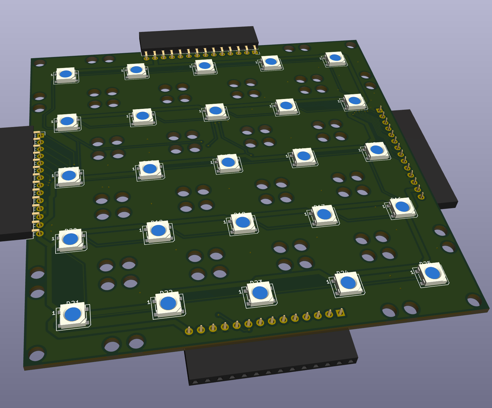
Wall is an open-source printed circuit board by rmingon, from the rmingon/led-wall repository on GitHub. It is a 2-layer board of 100 × 100 mm with 40 parts on 48 nets, routed with 761 tracks and 60 vias.
It is built around the AMS1117-3.3 and WS2812B. Its parts include 26 diodes, 5 connectors, 4 capacitors, 2 resistors and 2 ICs. It belongs with the RISC-V boards of this library.


A modular 5×5 WS2812B LED tile driven by a CH32V003 slave MCU.
Tiles share a simple 8-bit parallel bus + CLK + EN so a Raspberry Pi (or any MCU) can address many tiles and push pixel data quickly.
DATA0…DATA7, CLK, EN, optional RST/wall/
wall.kicad_pro
wall.kicad_pcb
wall.kicad_sch
wall.kicad_prl
/media/
wall_top_3d.jpeg
wall_bottom_3d.jpeg
wall_pcb.png
wall_schematic.png
/firmware/ # (placeholder) CH32V003 code
/tools/ # (placeholder) host examples (Raspberry Pi)
README.mdmedia/wall_top_3d.jpegmedia/wall_bottom_3d.jpegmedia/wall_pcb.pngmedia/wall_schematic.pngCH32V003F*P6 (labelled U1 in the schematic).
CLK and EN on PDx pins (see net labels in schematic)PA1/PA2 used for the WS2812 data output to the first LED in the chainRST net broken out (optional external reset)⚠️ Current budget: Each WS2812B can draw up to 40 mA at full-white.
One tile worst-case ≈ 25 × 40 mA = 1.5 A @ 5 V (plus margin).
Size your power rails accordingly and avoid sustained full-white if thermals are tight.
Each edge header is a 1×14 connector carrying power and the parallel bus.
| Pin | Signal | Notes |
|---|---|---|
| 1 | DATA0 | Parallel data bit 0 (MCU PC0) |
| 2 | DATA1 | (PC1) |
| 3 | DATA2 | (PC2) |
| 4 | DATA3 | (PC3) |
| 5 | DATA4 | (PC4) |
| 6 | DATA5 | (PC5) |
| 7 | DATA6 | (PC6) |
| 8 | DATA7 | (PC7) |
| 9 | CLK | Rising edge latch (EXTI7_0 IRQ) |
| 10 | EN | Tile enable / latch (PDx) |
| 11 | GND | Ground |
| 12 | GND | Ground (second pin for current) |
| 13 | +5V | LED power |
| 14 | +5V | LED power (second pin for current) |
Exact PDx assignments are labelled in the schematic nets; keep those in firmware defines so you can move them if the footprint changes.
Each frame is transmitted as a sequence of bytes clocked on PD2 rising edge while the slave samples D0–D7.
Frame format:
SOF0 SOF1 ADDR CMD LEN PAY[LEN] CRC0xA50x5A0xFF for broadcastADDR..CMD..LEN..PAY| CMD | Name | LEN | Payload description |
|---|---|---|---|
| 0x01 | SET_ALL_RGB | 3×N (75) | [R,G,B] triplets for all LEDs |
| 0x02 | SET_ONE_RGB | 4 | [index, R, G, B] (0–24 index) |
| 0x03 | FILL_RGB | 3 | [R, G, B] fill all LEDs |
| 0x04 | BOOT_TEST | 0 | Run built-in RGB test animation |
riscv-none-elf-gcc + openocd for WCH-LinkE).DATA[7:0], CLK, EN, LEDCLK while EN=1PAxBuild steps (outline):
/kicad/wall.kicad_pro to view hardware./wall_code/ in your IDE; set your tile address in main.c.Set all 25 LEDs to red (255,0,0):
A5 5A 12 01 4B FF 00 00 FF 00 00 ... (25 triplets) ... CRC0xA5 0x5A = SOF0x12 = target address0x01 = SET_ALL_RGB0x4B = 75 payload bytesCRC = computed over ADDR..PAYLOADhost.py in your IDE.Set all 25 LEDs to red (255,0,0):
A5 5A 12 01 4B FF 00 00 FF 00 00 ... (25 triplets) ... CRC0xA5 0x5A = SOF0x12 = target address0x01 = SET_ALL_RGB0x4B = 75 payload bytesCRC = computed over ADDR..PAYLOADCLK edges and that DATA[7:0] are stable at each edge while EN=1.Designed by RMINGON.
KiCad project files: kicad/wall.* (created with KiCad 9.0.3).
| Ref | Part | Notes |
|---|---|---|
| U1 | CH32V003F…P6 | 3.3 V RISC-V MCU |
| U3 | AMS1117-3.3 | 5 V → 3.3 V LDO |
| D1–D25 | WS2812B | 5 V addressable LEDs |
| D26, R4 | Status LED + 5 Ω–1 kΩ | (value per brightness; schematic shows R4 5 Ω) |
| J1–J4 | 1×14 headers | Bus + Power |
| C1–C3 | 10 µF/0.1 µF mix | Regulator & MCU decoupling |
Tweak values to match your inventory and regulator stability requirements (e.g., AMS1117 likes ≥10 µF on input/output).
| Qty | Value | Footprint | References |
|---|---|---|---|
| 25 | WS2812B | LED_SMD:LED_WS2812B_PLCC4_5.0x5.0mm_P3.2mm | D1, D2, D10, D11, D12, D13, D14, D15, D16, D17, D18, D19, D20, D21, D22, D23 +9 |
| 4 | C | Capacitor_SMD:C_0603_1608Metric | C1, C2, C3, C4 |
| 4 | Conn_01x14 | Connector_PinSocket_2.54mm:PinSocket_1x14_P2.54mm_Horizontal | J1, J2, J3, J4 |
| 2 | R_Small | Resistor_SMD:R_0603_1608Metric | R4, R5 |
| 1 | AMS1117-3.3 | Package_TO_SOT_SMD:SOT-223-3_TabPin2 | U3 |
| 1 | CH32V003FxPx | Package_SO:TSSOP-20_4.4x6.5mm_P0.65mm | U1 |
| 1 | Conn_01x01_Pin | TestPoint:TestPoint_Pad_D2.0mm | J5 |
| 1 | LED | LED_SMD:LED_0603_1608Metric | D26 |
| 1 | SW_Push | Button_Switch_SMD:SW_SPST_FSMSM | BTN1 |
It measures 100 × 100 mm and has 2 copper layers, 1.6 mm thick.
40 parts, built around the AMS1117-3.3 and WS2812B. The full list of its parts is on this page, with links to each part's symbol and footprint where PCBKit's library has them.
From the rmingon/led-wall repository on GitHub, at the commit this page was made from: the board is wall/wall.kicad_pcb and its schematic hardware/hardware.kicad_sch. PCBKit opens the board in the browser, with nothing to install.
Its repository states no licence, so its author keeps all rights: ask rmingon before reusing the design.
fossasia/pslab-hardware
PSLab Hardware Design and Schematics https://pslab.io

MycroftAI/hardware-mycroft-mark-II
Mycroft's Mark II Rpi mechanical, electrical and industrial designs


NuttyShell/NuttyBadge
NuttyBadge: A NuttyShell crafted multi-tool. Opensourced Hardawre and Software


Tomas-Kuchta-FPV/Open-ESPilot
An open-source project to develop a custom ESP32-based flight controller designed primarily for use with ArduPilot. Focused on affordability, flexibility, and ease of integration with various robotic and UAV platforms.

