2 layers155.7 × 96.1 mm
Raise right asym
Dygmalab/raise-right-asym
Licensed under CERN-OHL and distributed as is without any additional warranty or documentation.
566 parts1

 rljacobson/SpaceCadet14
Space Cadet Keyboard Schematic and PCB
SpaceCadet is an open-source printed circuit board by rljacobson, from the rljacobson/SpaceCadet repository on GitHub. It is a 2-layer board of 469 × 166.6 mm with 566 parts on 81 nets, routed with 3,097 tracks and 0 vias.
Its parts include 131 switches, 8 resistors, 6 capacitors, 3 connectors and 2 ICs. It belongs with the keyboards and input boards of this library.
This repo contains KiCAD source files and generated gerber files for the "Space Cadet" keyboard, reverse engineered from reference photos in May 2022. To my knowledge, this is the first and only reproduction of this keyboard in EDA form.
The board comes in three flavors:
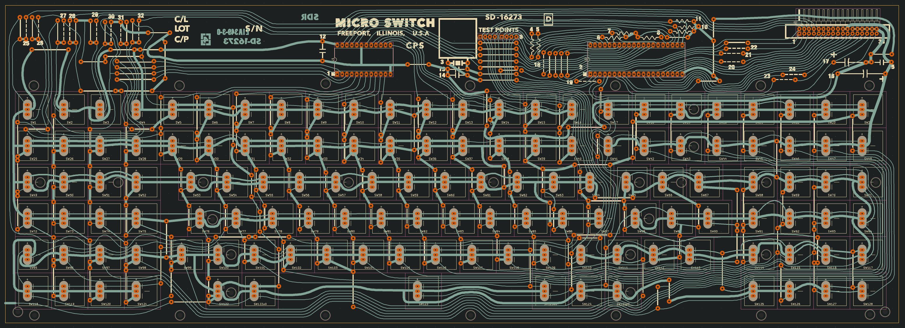
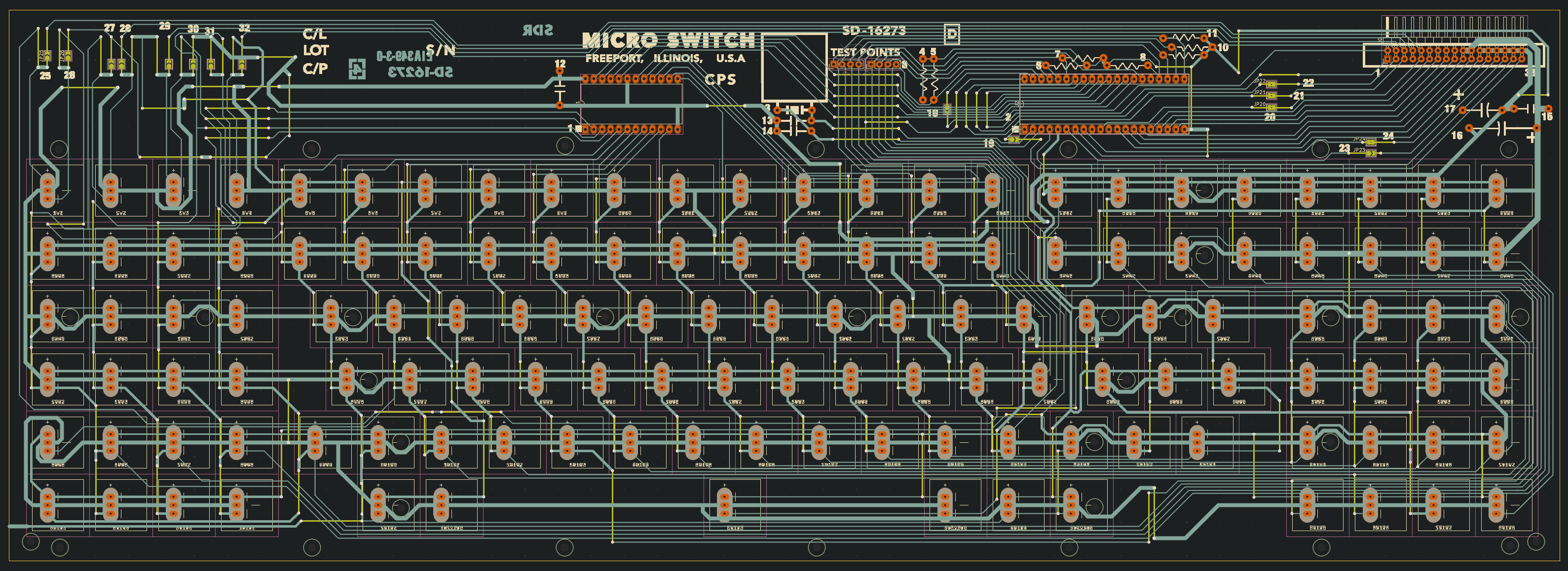
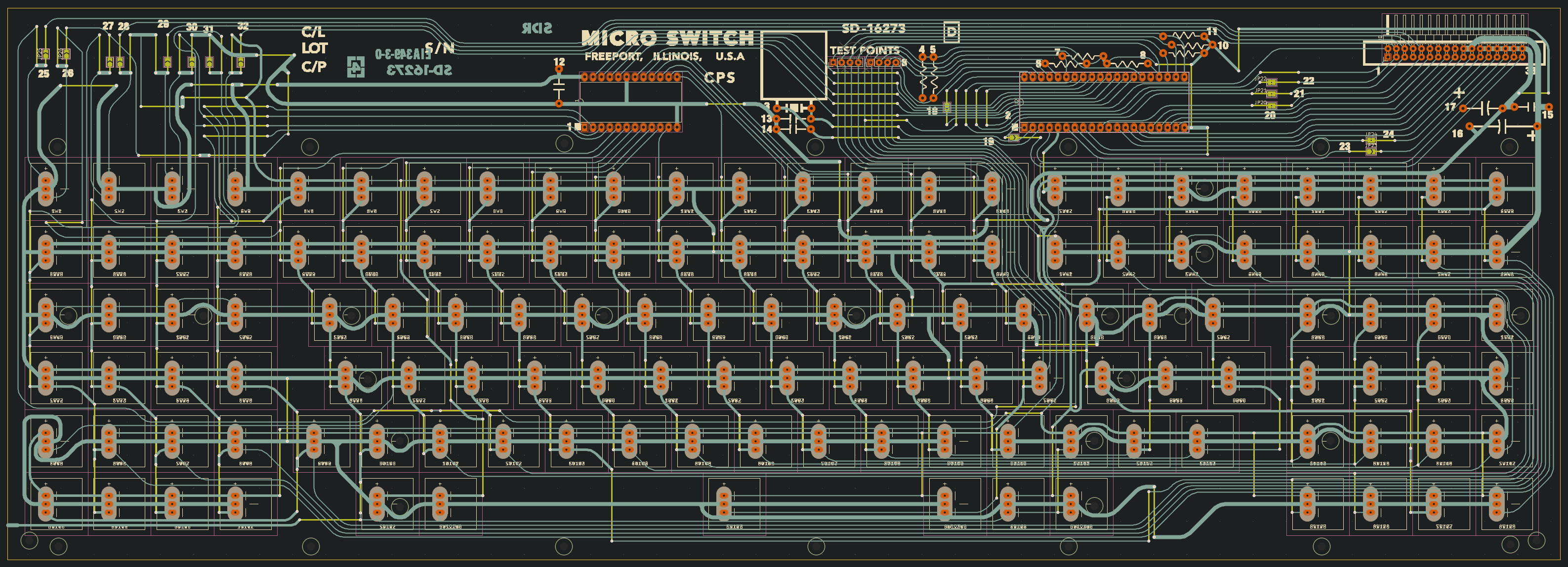
Variations #2 and #3 are in the Modern branch.
The design files were reverse engineered from a variety of reference materials. As quality reference materials were hard to get ahold of, I also include them here:

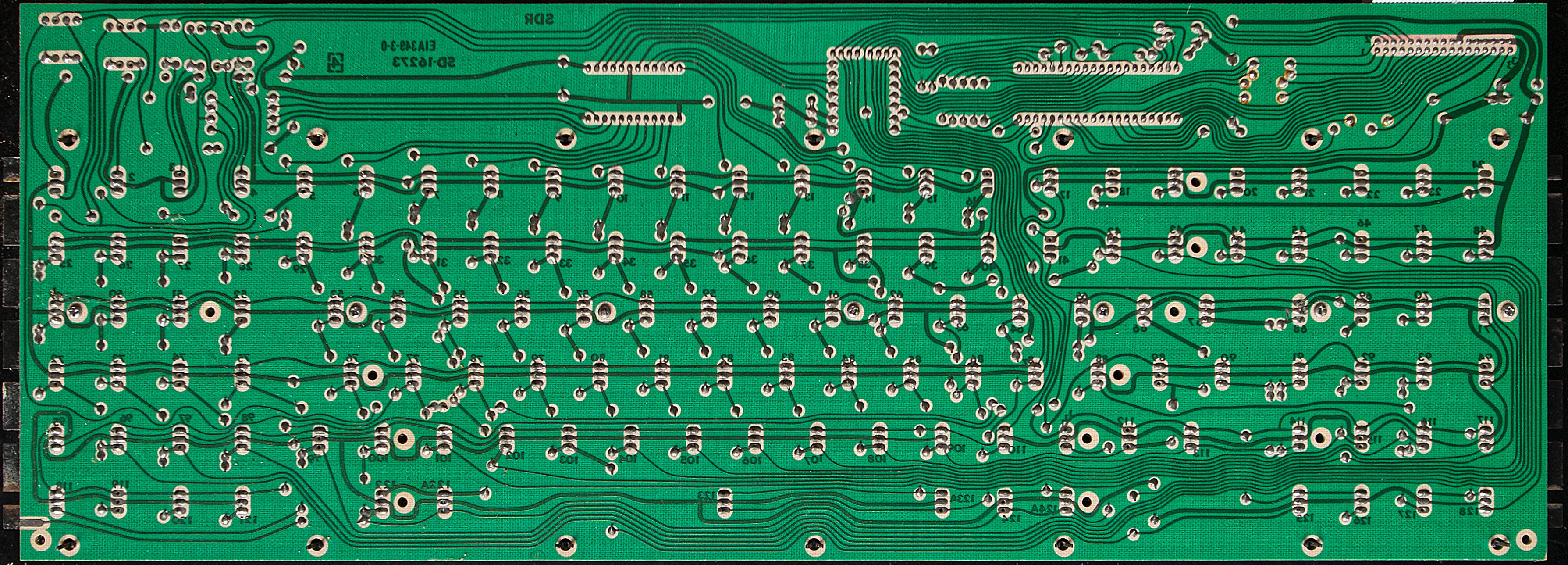
I am unable to find a reference for the entire front of the PCB without the key switches and panel obscuring most of the board. From the traces and vias visible on the back of the PCB, there are clearly many jumper wires on the front of the PCB the locations of which are easily determined.
These source files are Copyright © 2022 by Robert Jacobson. They are distributed under the terms of the CERN Open Hardware – Permissive license, also called the CERN-OHL-P v2 license. See LICENSE.txt for details.
| Qty | Value | Footprint | References |
|---|---|---|---|
| 379 | ThroughHole | ThroughHole | , , , , , , , , , , , , , , , +363 |
| 131 | SD_4B3E | Button_Switch_Keyboard:MicroSwitch_SD_Series_E | SW1, SW10, SW11, SW100, SW101, SW102, SW103, SW104, SW105, SW106, SW107, SW108, SW109, SW110, SW111, SW112 +115 |
| 8 | 1K | TestPoint:Two_Pad_Through_Hole_12.4mm | R4, R5, R6, R7, R8, R9, R10, R11 |
| 3 | 10pF | TestPoint:Two_Pad_Through_Hole_10.4mm | C12, C13, C14 |
| 2 | Conn_01x04 | Connector_PinHeader_2.54mm:PinHeader_1x04_P2.54mm_Vertical | J3_1, J3_2 |
| 1 | 15pF | TestPoint:Two_Pad_Through_Hole_10.4mm | C15 |
| 1 | 22uF 15v | TestPoint:Two_Pad_Through_Hole_20mm | C16 |
| 1 | 4.7uF 25v | TestPoint:Two_Pad_Through_Hole_12mm | C17 |
| 1 | 74LS154 | Package_DIP:DIP-24_W15.24mm_LongPads | U1 |
| 1 | 8048 | Package_DIP:DIP-40_W15.24mm_Socket_LongPads | U2 |
| 1 | Conn_02x17_Odd_Even | Connector_PinHeader_2.54mm:PinHeader_2x17_P2.54mm_Horizontal | J0 |
| 1 | Crystal 3.58MHz | TestPoint:Two_Pad_Through_Hole_10.4mm | Y3 |
| 1 | LOGO | Battery:silkscreen back | G*** |
| 1 | LOGO | Graphics_Text | G*** |
The 532 most common of 566 parts.
It measures 469 × 166.6 mm and has 2 copper layers, 1.6 mm thick.
566 parts. The full list of its parts is on this page, with links to each part's symbol and footprint where PCBKit's library has them.
From the rljacobson/SpaceCadet repository on GitHub, at the commit this page was made from: the board is SpaceCadet.kicad_pcb and its schematic SpaceCadet.kicad_sch. PCBKit opens the board in the browser, with nothing to install.
Its repository states no licence, so its author keeps all rights: ask rljacobson before reusing the design.
Dygmalab/raise-right-asym
Licensed under CERN-OHL and distributed as is without any additional warranty or documentation.


BoltzRnD/SmartPrintCoreH7x
STM32H7 based Robust and Open Source 3D Printer Mainboard

Roboy/HTC_Vive_Sensors
Schematics and PCB designs for our custom Vive sensors based on a quad op-amp chip rather than discrete transistors.


