2 layers43.9 × 27.7 mm

 rixnobis/ps1-port-tap
PS1 controller/memory card port pass-through with a logic analyser tap (KiCad)
Ps1-port tap is an open-source printed circuit board by rixnobis, from the rixnobis/ps1-port-tap repository on GitHub. It is a 2-layer board of 40 × 51 mm with 19 parts on 18 nets, routed with 40 tracks and 79 vias.
Its parts include 8 resistors and 3 connectors. It belongs with the sensors and measurement boards of this library.
A pass-through for one PlayStation controller or memory card port, with every line broken out to a 0.1" header for a logic analyser. Cut a controller extension cable in half, solder the console half to J1 and the device half to J2, and clip the analyser onto J3.
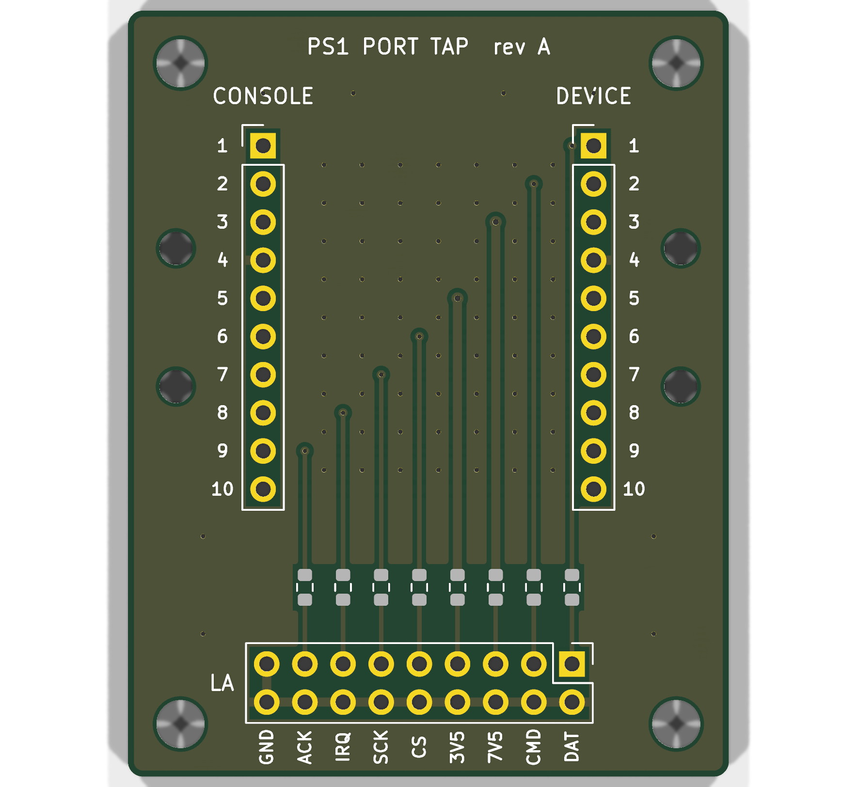
The PS1 port connector is proprietary, and I could not find a published drawing of it I would trust. The best public source is a forum post giving a 4 mm pitch, but its author traced the positions from a scaled photo. So this revision has no connector on the board: J1 and J2 are 1x10 rows at 2.54 mm with 1.0 mm holes, big enough for the cable's conductors. The M2 holes beside each row are for zip ties that hold the cable jacket. A board-mounted socket can come in a later revision, once someone has put calipers on a real one.
From psx-spx, docs/ps1/pinouts/controller-ports-and-memory-card-ports.md. Pins 1-9
are the port pins. Pin 10 carries the cable shield straight through and is not tapped.
Memory card slots have no IRQ (pin 8) and no shield.
| Pin | Signal | Pin | Signal | |
|---|---|---|---|---|
| 1 | DAT, data from device | 6 | /CS, port select | |
| 2 | CMD, data to device | 7 | SCK, clock | |
| 3 | +7.5V, rumble supply | 8 | /IRQ, lightgun | |
| 4 | GND | 9 | /ACK, acknowledge | |
| 5 | +3.5V, logic supply | 10 | shield |
The full table is also printed on the back silkscreen, so the cable can be wired from the board alone.
J3 is a 2x9 header. Odd pins carry the taps (DAT, CMD, 7V5, 3V5, CS, SCK, IRQ, ACK) and every even pin is GND, so each probe gets its own ground. The signal taps go through 100R, which keeps the analyser's lead capacitance off the bus; fit 0R if you want a transparent tap. The two supply taps go through 10k, so a probe clipped onto a rail cannot short it.
Two layers, 40 x 51 mm, routed by script and every run straight. Port line n crosses B.Cu from J1 pin n to J2 pin n. A tapped line drops through a via at its J3 column and runs straight down F.Cu to its resistor, and on to its J3 pin. Both layers are poured with GND, with stitching vias between the through-lines, so the copper there stays as stitched guard ground. The pour stops at a straight edge around each pad row, because between two header pads it can only form slivers; the GND pins inside those strips reach the pour through traces.
tools/check_geometry.py checks what DRC does not. It flags any bend sharper than
45 degrees, any segment shorter than its width, any trace narrower than its net class,
any dangling end and any overlapping segment. tools/crops.sh renders every pad row
and the resistor row at about 4x, in renders/crops/.
ps1-port-tap.kicad_sch, .kicad_pcb, .kicad_pro: KiCad 10 projectschematic.pdf, renders/: every copper and silk layer, plus 3D viewsfab/ps1-port-tap-gerbers.zip, fab/ps1-port-tap-bom.csv, fab/ps1-port-tap-cpl.csv:
ready for JLCPCB, with the resistors assembled and the headers hand-fitted. On the
JLC preview, check that the resistors sit square on their pads. LCSC lists C25804 (10k)
as out of stock right now; any 0603 10k works.Everything is generated from the scripts in tools/. tools/build.sh runs the whole
pipeline: schematic, ERC, placement and routing through the pcbnew Python API, pours,
DRC with schematic parity, the geometry check, renders, crops and fab outputs. It stops
on any ERC, DRC or geometry finding. Requires KiCad 10 (kicad-cli and the pcbnew
Python module), rsvg-convert and ImageMagick.
Not yet built or tested on hardware.
| Qty | Value | Footprint | References |
|---|---|---|---|
| 6 | 100 | Resistor_SMD:R_0603_1608Metric | R1, R2, R5, R6, R7, R8 |
| 4 | M3 | MountingHole:MountingHole_3.2mm_M3 | H1, H2, H3, H4 |
| 4 | ZIPTIE | MountingHole:MountingHole_2.2mm_M2 | H5, H6, H7, H8 |
| 2 | 10k | Resistor_SMD:R_0603_1608Metric | R3, R4 |
| 1 | CONSOLE | Connector_PinHeader_2.54mm:PinHeader_1x10_P2.54mm_Vertical | J1 |
| 1 | DEVICE | Connector_PinHeader_2.54mm:PinHeader_1x10_P2.54mm_Vertical | J2 |
| 1 | LA_TAP | Connector_PinHeader_2.54mm:PinHeader_2x09_P2.54mm_Vertical | J3 |

hackclub/OnBoard
💡 Join 1,000 teenagers and make your first PCB with a $100 grant!

polpo/picogus
Emulation of ISA sound cards and CD-ROM on Raspberry Pi Pico (GUS, SB/Adlib, MPU-401, Tandy, CMS, Panasonic CD-ROM) with USB mouse/joystick support


nkitanov/iaq_board
IAQ Board is a DIY (Do-It-Yourself) device for measuring internal air quality


Ardumower/ardumower
Develop an open source robotic lawn mower (HW+SW reference platform)

zmaker/arduino_cookbook
gli sketch del nuovo progetto Arduino Cookbook e dei video di YouTube
It measures 40 × 51 mm and has 2 copper layers, 1.6 mm thick.
19 parts. The full list of its parts is on this page, with links to each part's symbol and footprint where PCBKit's library has them.
From the rixnobis/ps1-port-tap repository on GitHub, at the commit this page was made from: the board is ps1-port-tap.kicad_pcb and its schematic ps1-port-tap.kicad_sch. PCBKit opens the board in the browser, with nothing to install.
Its repository states no licence, so its author keeps all rights: ask rixnobis before reusing the design.