2 layers103 × 30.5 mm

 riteshh27/IR-SENSOR-PCB
A KiCad hardware project for a simple IR (infrared) obstacle/proximity sensor module, featuring an IR emitter/receiver pair, a comparator threshold circuit, sensitivity adjustment, and status indication.
IR SENSOR is an open-source printed circuit board by riteshh27, from the riteshh27/IR-SENSOR-PCB repository on GitHub, published under the MIT licence. It is a 2-layer board of 51.1 × 15.5 mm with 9 parts on 7 nets, routed with 40 tracks and 0 vias.
Its parts include 3 resistors, 3 diodes, 1 IC and 1 connector. It belongs with the sensors and measurement boards of this library.
A KiCad hardware project for a simple IR (infrared) obstacle/proximity sensor module, featuring an IR emitter/receiver pair, a comparator threshold circuit, sensitivity adjustment, and status indication.
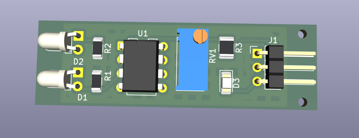
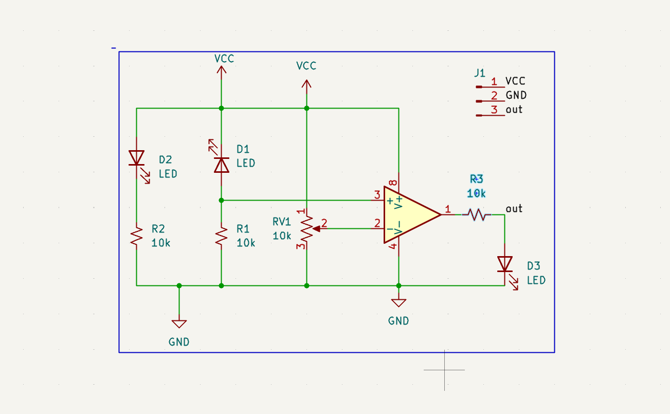
| Designator | Description | Footprint | Qty |
|---|---|---|---|
| D1 | IR receiver (photodiode/phototransistor) | LED_D3.0mm_Horizontal_O1.27mm_Z2.0mm_Clear | 1 |
| D2 | IR emitter LED | LED_D3.0mm_Horizontal_O1.27mm_Z2.0mm_Clear | 1 |
| D3 | Status LED | LED_1206_3216Metric | 1 |
| J1 | 3-pin header (VCC, GND, out) | PinHeader_1x03_P2.54mm_Horizontal | 1 |
| R1, R2 | Resistor, 10k | R_1206_3216Metric | 2 |
| R3 | Resistor, 10k | R_1210_3225Metric | 1 |
| RV1 | Potentiometer, 10k (sensitivity/threshold trim) | Bourns 3296W (vertical trimmer) | 1 |
| U1 | Single comparator (e.g. LM393/LM311) | DIP-8 (0.3", 7.62mm) | 1 |
| Pin | Function |
|---|---|
| 1 | VCC |
| 2 | GND |
| 3 | out (digital detection signal) |
| Top Copper (annotated) | Bottom Copper |
|---|---|
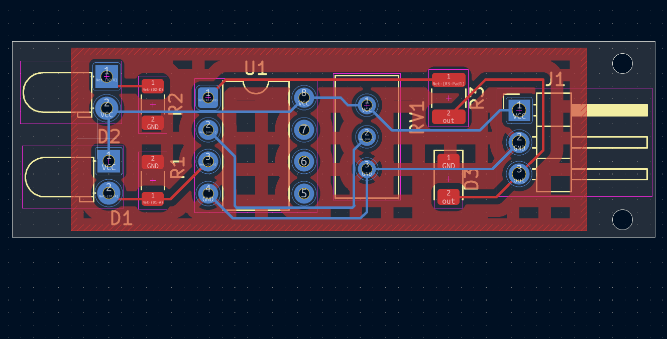 | 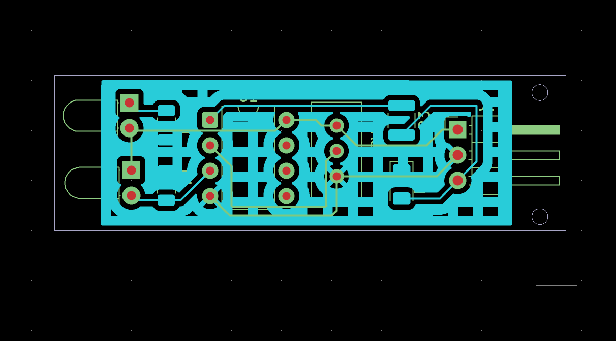 |
| 3D Top | 3D Bottom |
|---|---|
| 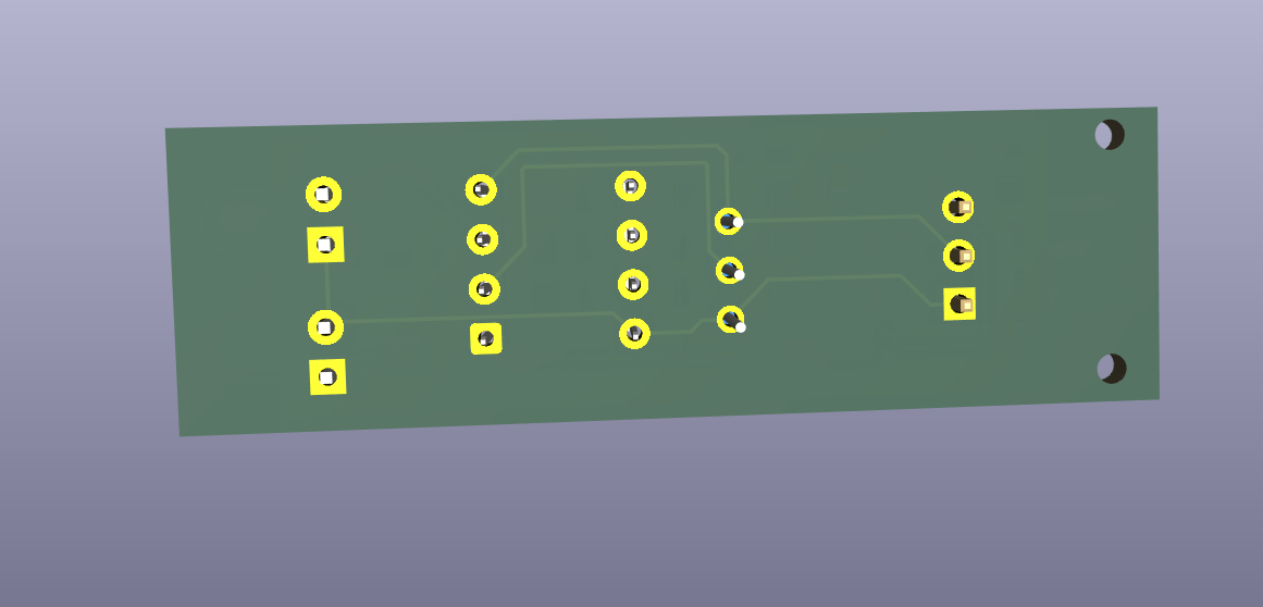 |
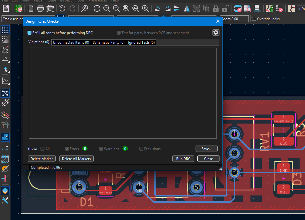
Passed with 0 violations:
| File | Description |
|---|---|
IR_SENSOR.kicad_pro | KiCad project file |
IR_SENSOR.kicad_sch | Schematic |
IR_SENSOR.kicad_pcb | PCB layout |
IR_SENSOR.kicad_prl | Local project settings (layer visibility etc.) |
IR_SENSOR.csv | Bill of materials (BOM) |
IR_SENSOR.rpt | KiCad DRC/electrical rules report |
IR_SENSOR_report.txt | PCB statistics report (board area, pads, vias) |
docs/images/ | Schematic, layout, 3D render, and DRC screenshots |
git clone https://github.com/riteshh27/IR-SENSOR-PCB.gitIR_SENSOR.kicad_pro in KiCad to view/edit the schematic and PCB layout.To generate Gerber files for fabrication:
See LICENSE for details.
| Qty | Value | Footprint | References |
|---|---|---|---|
| 2 | 10k | Resistor_SMD:R_1206_3216Metric | R1, R2 |
| 2 | LED | LED_THT:LED_D3.0mm_Horizontal_O1.27mm_Z2.0mm_Clear | D1, D2 |
| 1 | 10k | Resistor_SMD:R_1210_3225Metric | R3 |
| 1 | 10k | Potentiometer_THT:Potentiometer_Bourns_3296W_Vertical | RV1 |
| 1 | LED | LED_SMD:LED_1206_3216Metric | D3 |
| 1 | ~ | Package_DIP:DIP-8_W7.62mm | U1 |
| 1 | ~ | Connector_PinHeader_2.54mm:PinHeader_1x03_P2.54mm_Horizontal | J1 |
It measures 51.1 × 15.5 mm and has 2 copper layers, 1.6 mm thick.
9 parts. The full list of its parts is on this page, with links to each part's symbol and footprint where PCBKit's library has them.
From the riteshh27/IR-SENSOR-PCB repository on GitHub, at the commit this page was made from: the board is IR_SENSOR.kicad_pcb and its schematic IR_SENSOR.kicad_sch. PCBKit opens the board in the browser, with nothing to install.
Its repository publishes it under the MIT licence: you may reuse it on that licence's terms (keep the author's notice, and for a copyleft licence share your changes alike).


FrameworkComputer/ExpansionCards
Reference designs and documentation to create Expansion Cards for the Framework Laptop

VoronDesign/Voron-Hardware
Cool Hardware designed by the Voron Design group

hackclub/OnBoard
💡 Join 1,000 teenagers and make your first PCB with a $100 grant!


adamws/kicad-kbplacer
KiCad plugin for automatic keyboard's key placement and routing