4 layers243.8 × 171.5 mm

 retro16/acsi2stm212
Atari ST ACSI to SD card converter with a STM32
ACSI2STM MegaSTE is an open-source printed circuit board by retro16, from the retro16/acsi2stm repository on GitHub, published under the GPL-3.0 licence. It is a 2-layer board of 125 × 58 mm with 17 parts on 47 nets, routed with 168 tracks and 10 vias.
It is built around the GSD090012SEU. Its parts include 3 connectors, 2 capacitors, 1 IC and 1 diode. It belongs with the retro computing and games boards of this library.
This a KiCAD (6.0) design to host an ACSI2STM directly inside an Atari Mega STE using the internal connector. The PCB has been designed to accomodate version 2.x and 3.x of ACSI2STM (aka V2) but also the old V1 design.
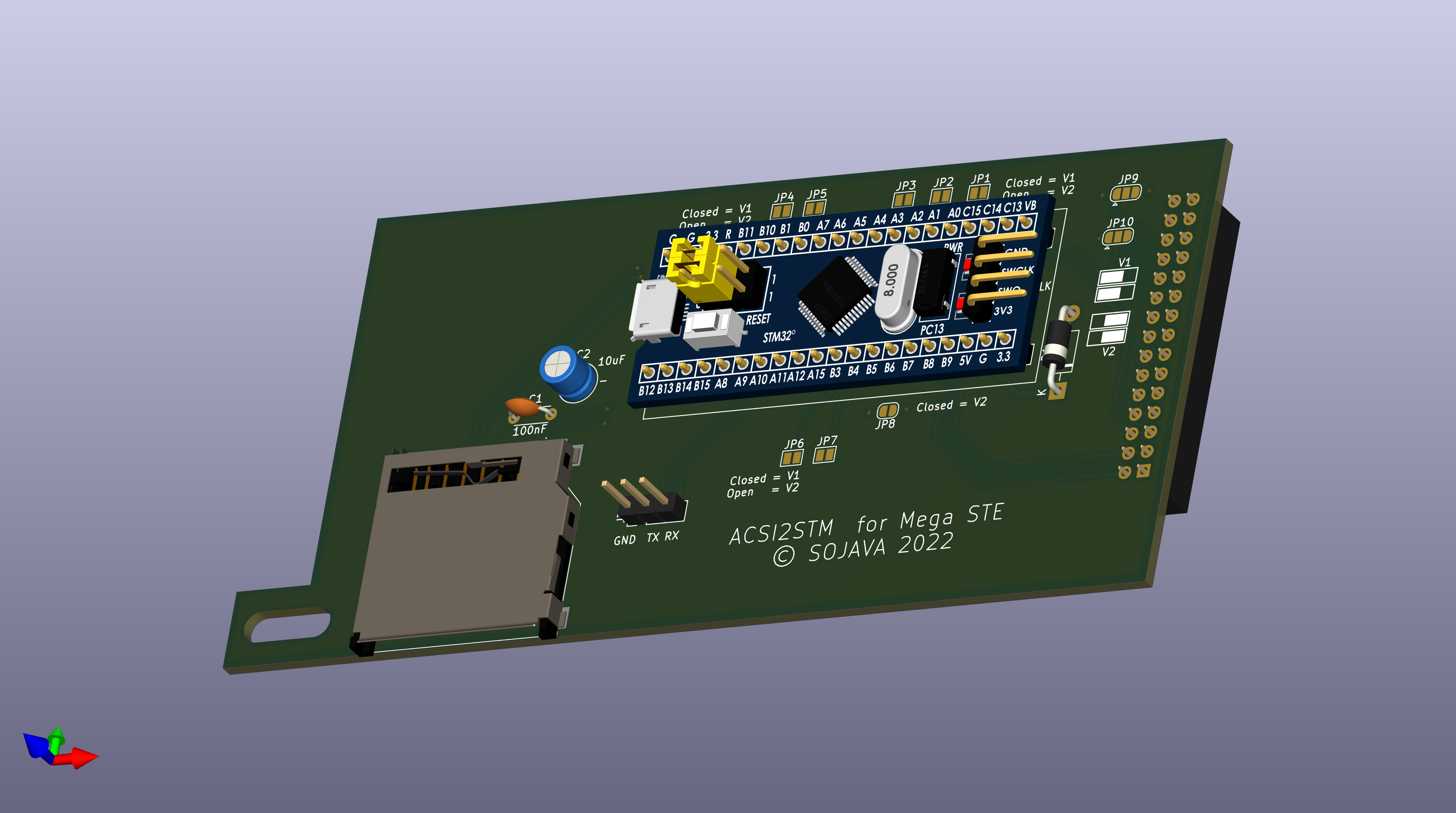
Configuration is done by simple solder bridges on the pads, instructions are also written on PCB.
A male 3 pin header is optional and only required if you want to program the STM32 without removing it from the Atari. The RX and TX marking correspond to the STM32 pins A10 an A09, to program the STM32 connect the board's RX to your USB-TTL TX and the board's TX to your USB-TTL-RX:
| USB-TTL | ACSI2STM |
|---|---|
| GND | GND |
| RX | TX |
| TX | RX |
In order to update the STM32:
:warning: Although the diode should avoid USB power from flowing back to the Mega STE, I haven't tested USB plugged-in while the MegaSTE is powered on. :warning:
| Qty | Value | Footprint | References |
|---|---|---|---|
| 7 | Close = V1 | Jumper:SolderJumper-2_P1.3mm_Open_Pad1.0x1.5mm | JP1, JP2, JP3, JP4, JP5, JP6, JP7 |
| 1 | 100nF | Capacitor_THT:C_Disc_D4.3mm_W1.9mm_P5.00mm | C1 |
| 1 | 10uF | Capacitor_THT:C_Radial_D5.0mm_H5.0mm_P2.00mm | C2 |
| 1 | 1N5817 | Diode_THT:D_DO-41_SOD81_P10.16mm_Horizontal | D1 |
| 1 | ACK Jumper | Jumper:SolderJumper-3_P1.3mm_Open_RoundedPad1.0x1.5mm | JP10 |
| 1 | BluePill | footprints:YAAJ_BluePill_1 | U1 |
| 1 | Conn_01x03_Male | Connector_PinHeader_2.54mm:PinHeader_1x03_P2.54mm_Vertical | J3 |
| 1 | GSD090012SEU | SamacSys_Parts:GSD090012SEU | J2 |
| 1 | Mega STE Internal ACSI | Connector_PinSocket_2.54mm:PinSocket_2x15_P2.54mm_Vertical | J1 |
| 1 | RST Jumper | Jumper:SolderJumper-2_P1.3mm_Open_RoundedPad1.0x1.5mm | JP8 |
| 1 | XHDINT Jumper | Jumper:SolderJumper-3_P1.3mm_Open_RoundedPad1.0x1.5mm | JP9 |
It measures 125 × 58 mm and has 2 copper layers, 1.6 mm thick.
17 parts, built around the GSD090012SEU. The full list of its parts is on this page, with links to each part's symbol and footprint where PCBKit's library has them.
From the retro16/acsi2stm repository on GitHub, at the commit this page was made from: the board is pcb/MegaSTE Internal/ACSI2STM MegaSTE.kicad_pcb and its schematic pcb/MegaSTE Internal/ACSI2STM MegaSTE.kicad_sch. PCBKit opens the board in the browser, with nothing to install.
Its repository publishes it under the GPL-3.0 licence: you may reuse it on that licence's terms (keep the author's notice, and for a copyleft licence share your changes alike).

Neotron-Compute/Neotron-Common-Hardware
Contains KiCad footprints and symbols shared across multiple Neotron projects.


KirtiChickamath/ESP32-IoT-sensor-board
ESP32- IoT sensor board. 4-layer PCB, designed in KiCad . Features LiPo charging, USB-C, SPI flash, SD card, BME280, and more.


Ankithkumarsingh/ESP32-custom-sensor-board
This PCB contains the power supply unit, ESP32 module as compute, microphone sensor, light sensing sensor, SDCard module for data logging.

aryan-asit/Telemetry-iot-project
In this project , a 4 layer custom pcb is made for Telematics

ddennis18/ESP32-IoT-DevBoard
An ESP32-C3 based IoT controller board designed in KiCad. The board combines wireless control, sensor interfaces, local storage, audio/light sensing, USB connectivity, and single-cell Li-ion battery support on a compact…