2 layers38.6 × 15.7 mm
LIPS V3.2
milar111/L.I.P.S.
OpenSource Affordable SipAndPuff device: Linear Interface for Paralysis Support
21 parts13
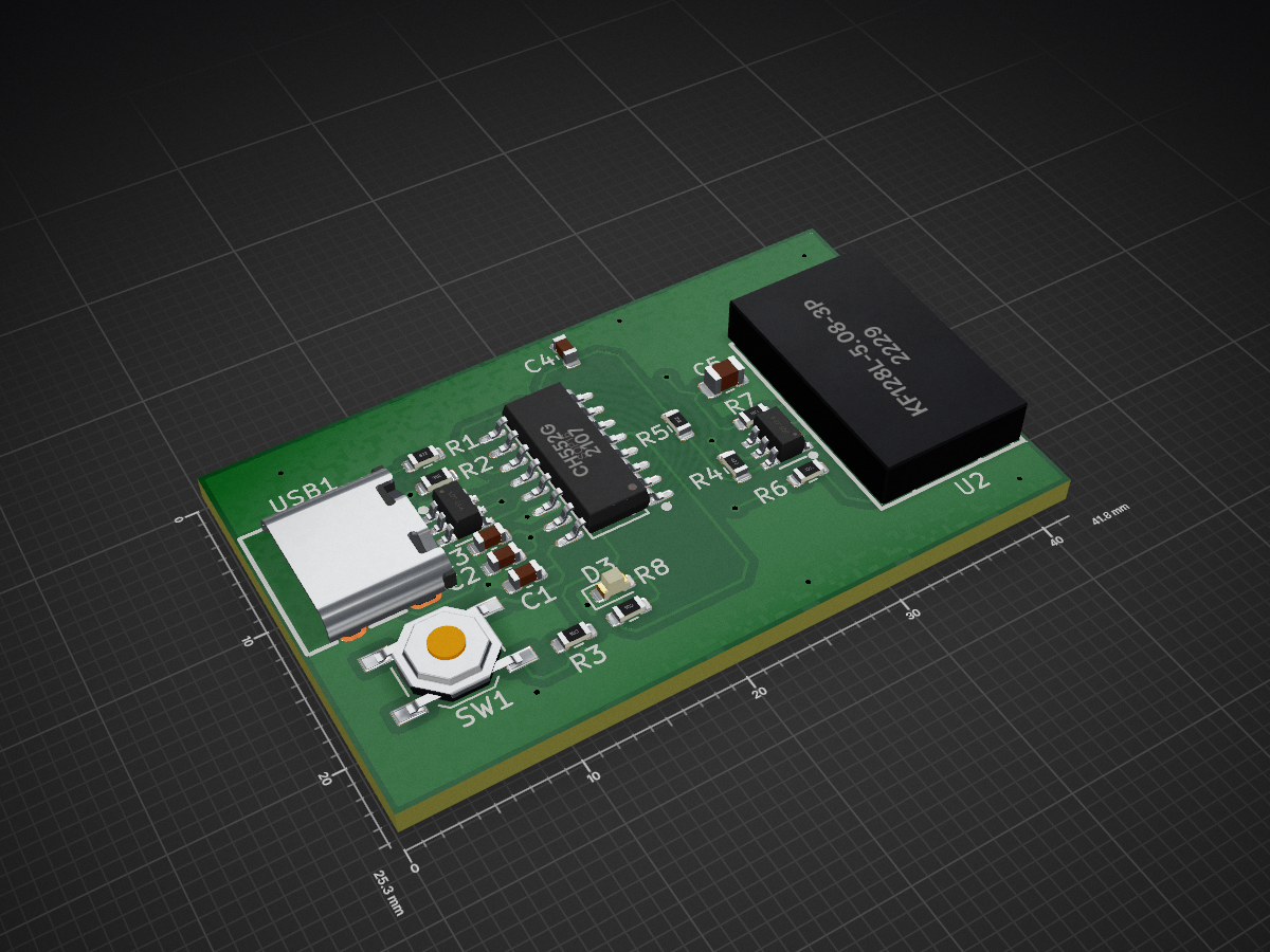
 recepbugra24/usb-button-controller
A minimal USB HID keyboard board that reads two externally wired buttons and sends keystrokes to a host computer. No drivers required — the host enumerates it as a standard keyboard.
Usb button controller is an open-source printed circuit board by recepbugra24, from the recepbugra24/usb-button-controller repository on GitHub. It is a 2-layer board of 41.8 × 25.3 mm with 20 parts on 26 nets, routed with 187 tracks and 21 vias.
It is built around the CH552G, KF128L-5.08-3P and USBLC6-2SC6. Its parts include 8 resistors, 5 capacitors, 3 diodes, 2 ICs and 1 switch. It belongs with the 8051 (CH55x, STC, AT89) boards of this library.


A minimal USB HID keyboard board that reads two externally wired buttons and sends keystrokes to a host computer. No drivers required — the host enumerates it as a standard keyboard.
Designed around the WCH CH552G, an 8-bit MCU with an integrated USB device controller, on-chip 24 MHz oscillator and on-chip 5 V to 3.3 V regulator. This removes the crystal, load capacitors, reset network and programming header that a comparable AVR design would need, and cuts the controller cost from roughly $4.70 to $0.31 per unit.
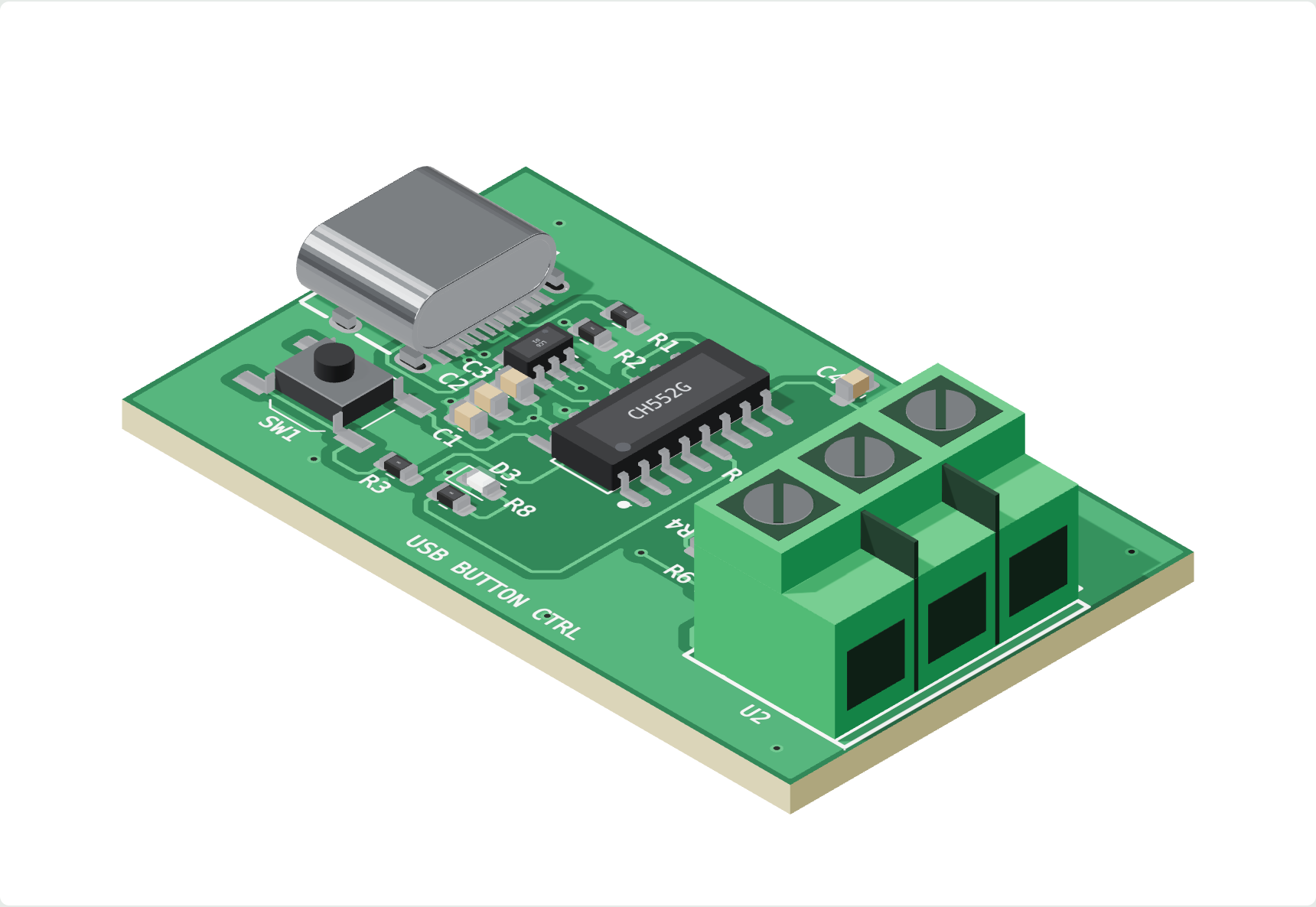
An interactive version is in docs/3d-viewer.html (open it in a browser).
| MCU | WCH CH552G (SOP-16) |
| Interface | USB 2.0 Full Speed, USB-C connector |
| Inputs | 2 buttons, wired off-board via screw terminal |
| Power | Bus powered, ~20 mA |
| Board | 41.8 × 25.25 mm, 2 layers, 1.6 mm FR-4 |
| Assembly | Single sided (top), SMD |
USB. Both differential pairs of the USB-C receptacle are tied together so the cable works in either orientation. CC1 and CC2 each carry a 5.1 kΩ pulldown to advertise the board as a sink; without them the host supplies no power. A USBLC6-2SC6 clamps ESD on D+/D- as close to the connector as layout allows.
Button inputs. Each channel has a 4.7 kΩ pull-up so the input never floats, a 1 kΩ series resistor and a 100 nF capacitor forming a low-pass filter with a 0.1 ms time constant, and a second USBLC6-2SC6 protecting against discharge carried in on the button wiring. The filter suppresses contact bounce in hardware; firmware adds a short debounce window on top.
Programming. The CH552G ships with a USB bootloader in ROM. Holding SW1 while plugging in pulls D+ to V33 through a 10 kΩ resistor, which puts the chip into bootloader mode. No external programmer is needed.
Ground. Copper pours on both layers, stitched with vias. The pour under the USB pair is kept unbroken to hold the differential impedance steady.
usb-button-controller.kicad_sch     schematic
usb-button-controller.kicad_pcb     board layout
usb-button-controller.kicad_pro     project file
docs/                   isometric render and interactive 3D viewer
gerber/                 fabrication output
  *.gtl *.gbl           copper layers
  *.gts *.gbs           solder mask
  *.gto *.gbo           silkscreen
  *.gm1                 board outline
  *.drl                 drill file
  BOM_jlcpcb.csv        bill of materials with LCSC part numbers
usb-button-controller-all-pos.csv component placementBuilt for JLCPCB with assembly. Upload the gerber archive, then the BOM and
placement files from gerber/.
Settings: 2 layers, 1.6 mm, HASL, top-side assembly. Enable Confirm Parts Placement — KiCad and JLCPCB do not always agree on the zero-rotation reference for SOT-23 and SOP packages, and the preview is where a misoriented part gets caught.
All passives, the LED and the tactile switch are JLCPCB Basic parts. The CH552G, USB-C receptacle, USBLC6-2SC6 and screw terminal are Extended parts and carry a per-part setup fee.
Built with ch55xduino in the Arduino IDE. Add this board manager URL:
https://raw.githubusercontent.com/DeqingSun/ch55xduino/ch55xduino/package_ch55xduino_mcs51_index.jsonInstall CH55x Boards, select CH552 Board, and pick a USB setting that reserves RAM for HID. Pin mapping:
| Function | Port | Arduino pin |
|---|---|---|
| Button 1 | P3.3 | 33 |
| Button 2 | P3.4 | 34 |
| Status LED | P1.7 | 17 |
A blank chip enters the bootloader on its own, so the first upload needs no button press. Later uploads are triggered automatically unless the running firmware has locked up the USB stack, in which case hold SW1 and replug.
Not yet verified in hardware — no board has been built from these files.
Not yet chosen. Add a LICENSE file before sharing this publicly.
| Qty | Value | Footprint | References |
|---|---|---|---|
| 3 | 100nF | Capacitor_SMD:C_0603_1608Metric | C1, C2, C4 |
| 3 | 1k | Resistor_SMD:R_0603_1608Metric | R5, R7, R8 |
| 2 | 4.7k | Resistor_SMD:R_0603_1608Metric | R4, R6 |
| 2 | 5.1k | Resistor_SMD:R_0603_1608Metric | R1, R2 |
| 2 | USBLC6-2SC6 | easyeda2kicad:SOT-23-6_L2.9-W1.6-P0.95-LS2.8-BL | D1, D2 |
| 1 | 100nF | Capacitor_SMD:C_0805_2012Metric | C5 |
| 1 | 10k | Resistor_SMD:R_0603_1608Metric | R3 |
| 1 | 10uF | Capacitor_SMD:C_0603_1608Metric | C3 |
| 1 | CH552G | easyeda2kicad:SOP-16_L10.0-W3.9-P1.27-LS6.0-BL | U1 |
| 1 | KF128L-5.08-3P | easyeda2kicad:CONN-TH_3P-P5.08_KF128L-5.08-3P | U2 |
| 1 | LED | LED_SMD:LED_0603_1608Metric | D3 |
| 1 | SW_Push | Button_Switch_SMD:SW_SPST_TL3342 | SW1 |
| 1 | TYPE-C 16PIN 2MD | easyeda2kicad:USB-C-SMD_TYPE-C-16PIN-2MD-073 | USB1 |
It measures 41.8 × 25.3 mm and has 2 copper layers, 1.6 mm thick.
20 parts, built around the CH552G, KF128L-5.08-3P and USBLC6-2SC6. The full list of its parts is on this page, with links to each part's symbol and footprint where PCBKit's library has them.
From the recepbugra24/usb-button-controller repository on GitHub, at the commit this page was made from: the board is usb-button-controller.kicad_pcb and its schematic usb-button-controller.kicad_sch. PCBKit opens the board in the browser, with nothing to install.
Its repository states no licence, so its author keeps all rights: ask recepbugra24 before reusing the design.
milar111/L.I.P.S.
OpenSource Affordable SipAndPuff device: Linear Interface for Paralysis Support

TECHOTAKU182/Pilot-Light
本版与 ../../enclosure/sl25trafficrevb/ 外壳配套,取代 Rev A 的偏上小灯珠设计。PCB 正面只有一颗位于几何中心的 WS2812B-V5,其他电子元件和 USB-C 均在背面。 板框仍为 25×25 mm,双层、1.6 mm 厚,两个 M2 孔的位置保持原接口。


gowenrw/BSidesDFW_2019_Badge
This is where all the files for the BSidesDFW 2019 Badge will be stored. This includes code and art and cab and fab files. All the things.