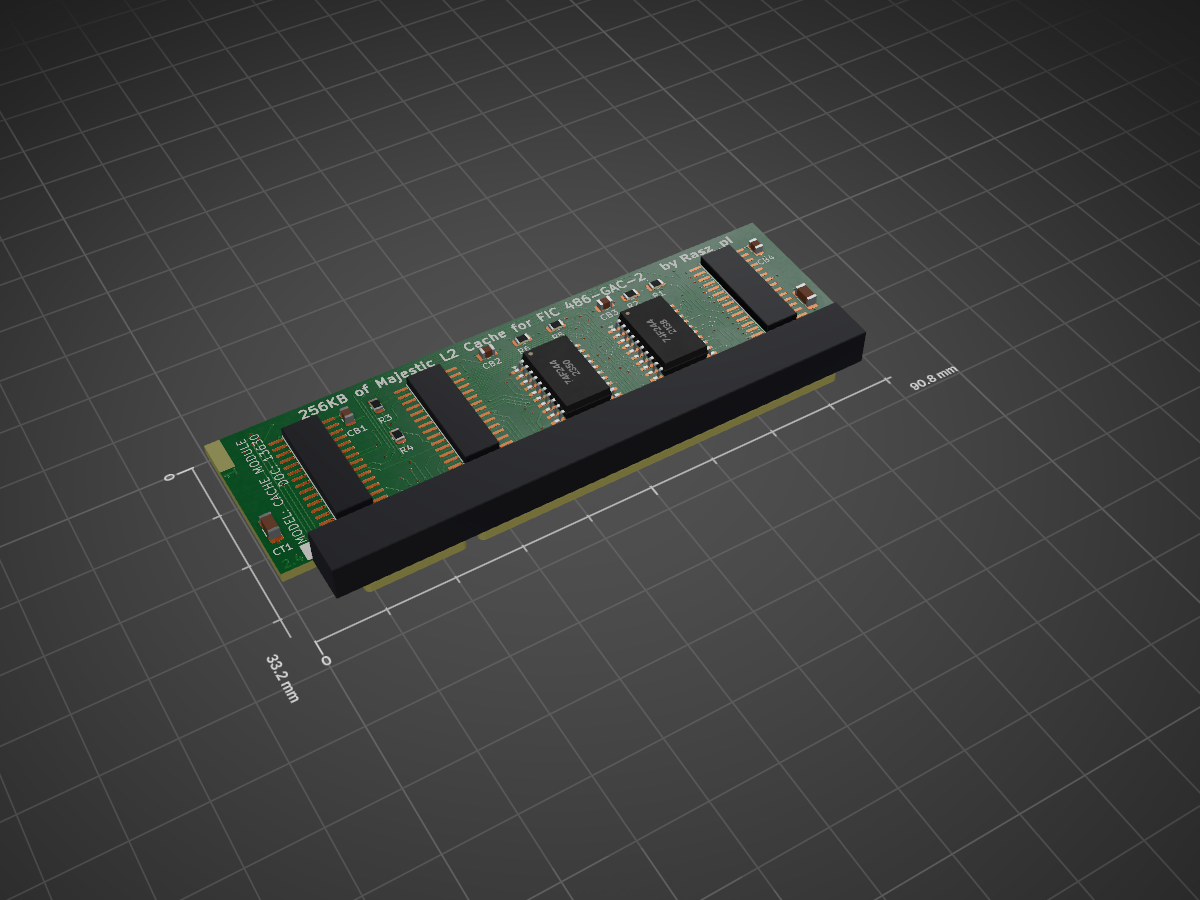
FIC-486-GAC-2 Cache Module reproduction
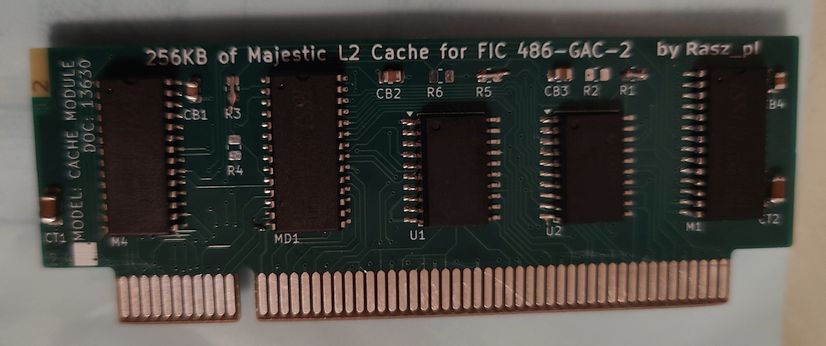
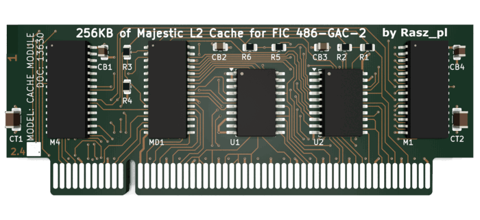
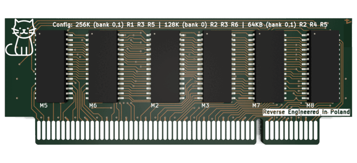
Reverse Engineered non standard 256K L2 Cache Module for use in:
- AT&T GLOBALYST 510 = NCR 3228 = FIC 486-GAC-2
- AT&T GLOBALYST 515 = NCR 3232 = FIC 486-GAC-2
Potentially also:
- AT&T Globalyst 520 = NCR 3238 = FIC 486-PAK-3/Vogons: What´s wrong with this FIC 486 PAK-3 ?? needs confirmation
- AT&T Globalyst 530 = NCR 3338 = FIC 486-PAK-3 needs confirmation
- NCR 3231
- AT&T Globalyst 525 = NCR 3253
Incompatible platforms also reusing VLB slot for Cache:
- AT&T
- pre 1993 Globalyst name change NCR MODEL 3230 (A4923 ISA) Uses VLB slot form factor, but in an edge connector form Vogons: NCR 3230-7020 486 DX 33 System - Cache question?
- Globalyst 550 = NCR 3246
- Globalyst 575 = NCR 3347 both use 517-0002811
- Compaq
- ProLinea 4/66 (164560-001)
- ProLinea MT/833CDS/850/850CDS/860CDS/866 (197023-001)
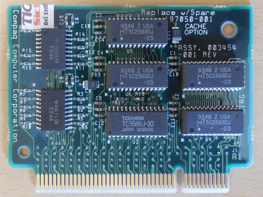
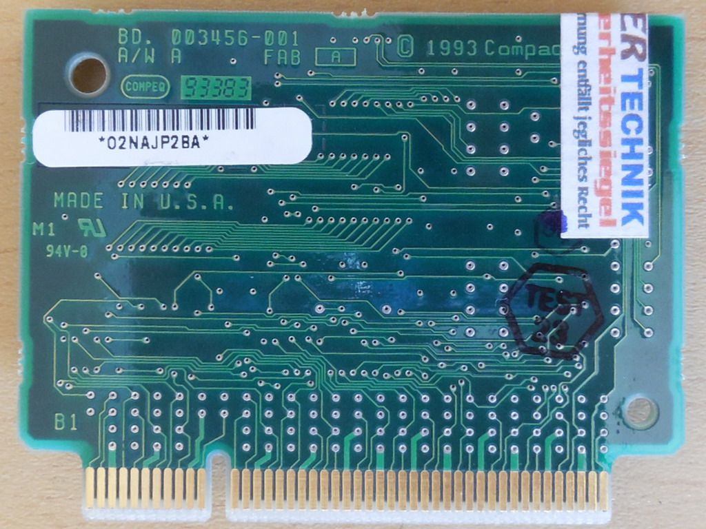
- Presario 700-900 series (171009-001) all three use 128KB 197005-001 (003670-001) front back in slot or 128KB 197050-001 (003454-001) front back. 100% working DIY 256KB/1MB Replacement by sander wichers inspired by this project :)
- Prosignia VS uses Sony CXK784862Q-33 based 256KB 194380-001 front back
- DESKPRO XE 486 uses Sony CXK784862Q-33 based 256KB Kingston KTC-4358 front in slot. Maybe 194380-001 compatible?
- Deskpro/i Family 3 uses Intel A82485-33 based 64KB 141345-001 (002581)
- Deskpro/i Family 4 uses Intel A82485-33 based 64KB 141477-001 (002754) front back
- HP Vectra VE 4 uses 256KB HP D2465A/IDT 7MP6193 front back
- HPE NetServer LC 5/166 (D4861AR) uses 256KB HP D3322A/IDT 7MP6152 (HP 0960-0899) front
- Olivetti M4 454 S uses 128KB CYM9236 and 256KB CYM9237PB front back with slot
- Siemens Nixdorf FD200 D882 uses 256KB CYM9252PB front back and unknown 128KB one.
Resources
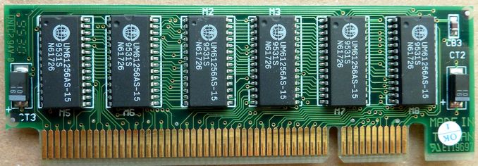
Pictures of the original "DOC: 13630" "ASSY: 008-0078204 A" Cache module:
rev 2 front 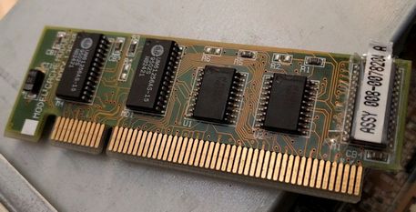
rev 2.1 front 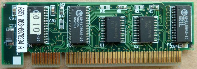 , back
plugged into FIC 486-GAC-2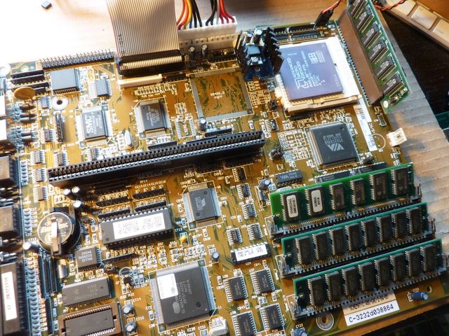
Vogons: FIC 486-GAC-2 proprietary cache module - open source reproduction Completed thread:
majestyk: "FIC sold two different versions with different pinouts (and the same "VLB"-socket). Only the one in the pictures works on a 486-GAC2 and a few other FIC mainboards."
This project was only possible with help provided by majestyk - owner of this very rare Cache module, and RockstarRunner - FIC 486-GAC-2 owner looking for said Cache module. Huge thanks for taking time to capture high resolution pictures and validating progress with measurements.
UMC UM61256A 32K x 8 Static RAM datasheet
VESA VLB slot pinout VESA VLB slot dimensions
Status
100%. Manufactured and tested. Preliminary design took 8 days. Fixes after assembling first prototype 2 days.
Progress report
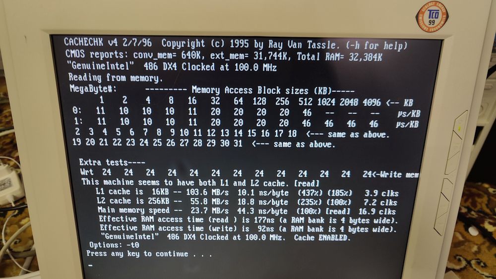
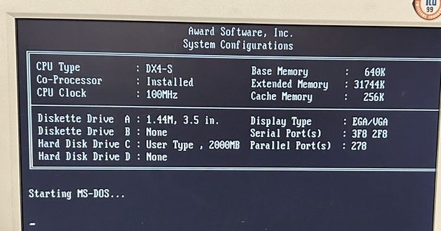
4/19/2024: Rev 2.4 assembled by swapping components from Rev 2.2. CACHECHK screenshot.
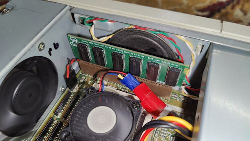
4/15/2024: Rev 2.4 'Pcbs turned up! We have edge connectors this time 😆'
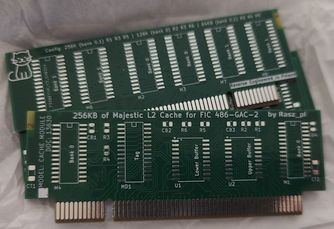
3/23/2024: Final Rev 2.4. Reworked SRAM footprint for easier hand soldering, slightly optimized capacitor placement.
2/29/2024: Final Rev 2.3. Slightly thicker tracks and silkscreen text, additional clearance work. Shrank from initial prototype, should be almost equal height of original. Height when inserted 26.3mm, height including slot 33.6mm.
2/28/2024: Prototypes assembled after sanding off soldermask from edge slot contacts, didnt work at first try. Turns out I swapped few power/ground pins in the connector resulting in dead short. Great sleuthing by Miisalo uncovered this mishap, after cutting bad connections we have sucessfull boot.
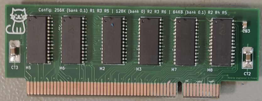
2/27/2024: Prototypes arrived. Who can spot the problem?
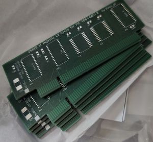
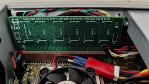
Will require some finessing with sandpaper to uncover edge slot pads :)
2/11/2024: 99% done, ERC&DRC 0 errors 0 warnings. Footprints should be correct now. Gerbers sent for manufacturing.
2/8/2024: 95% there, 0 errors, 7 Warnings. 5 connections missing, 11 guesses and assumptions on U1 U2 and some more on common lines.
2/6/2024: 90% there, 0 errors 18 warnings. Just a couple tracks left.
2/5/2024: 80% there, 0 drc errors, 62 violations. Still bad footprints and I havent gotten around to fixing power/ground pins. Whats left is figuring LS244 address buffering mapping, TAG ram address and output pins to edge mapping, WE/CE/OE mapping to edge.
2/4/2024: Very VIP, only about 50% there at the moment.
02/3/2024: Project start. Figuring out how to make edge connector footprint, searching for SOJ-28L footprint.
Work for hire
Interested in having a piece of hardware reverse engineered/cloned? Drop me an email.