2 layers116.8 × 30 mm
Type d
google/mozc-devices
Circuit diagrams and firmware source code for Gboard DIY keyboards
14 parts3kApache-2.0
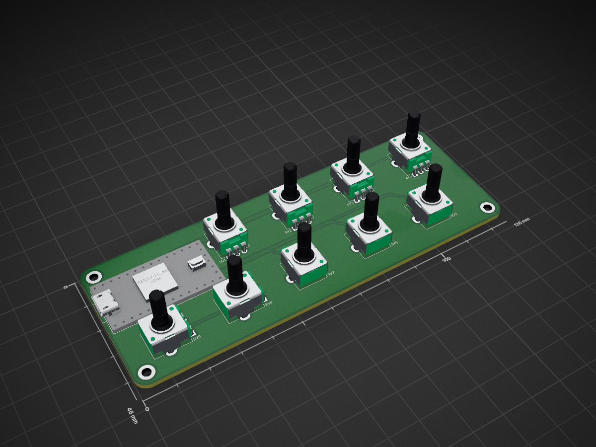
 ramphands/bleachedplusplus17
slightly expanded and simplified version of the original Bleached by andr-ew
Bleachedplusplus is an open-source printed circuit board by ramphands, from the ramphands/bleachedplusplus repository on GitHub, published under the GPL-3.0 licence. It is a 2-layer board of 126 × 46 mm with 14 parts on 27 nets, routed with 46 tracks and 0 vias.
It belongs with the NXP (LPC, Kinetis, i.MX RT) boards of this library.
slightly expanded and simplified version of the original Bleached PCB design by andr-ew
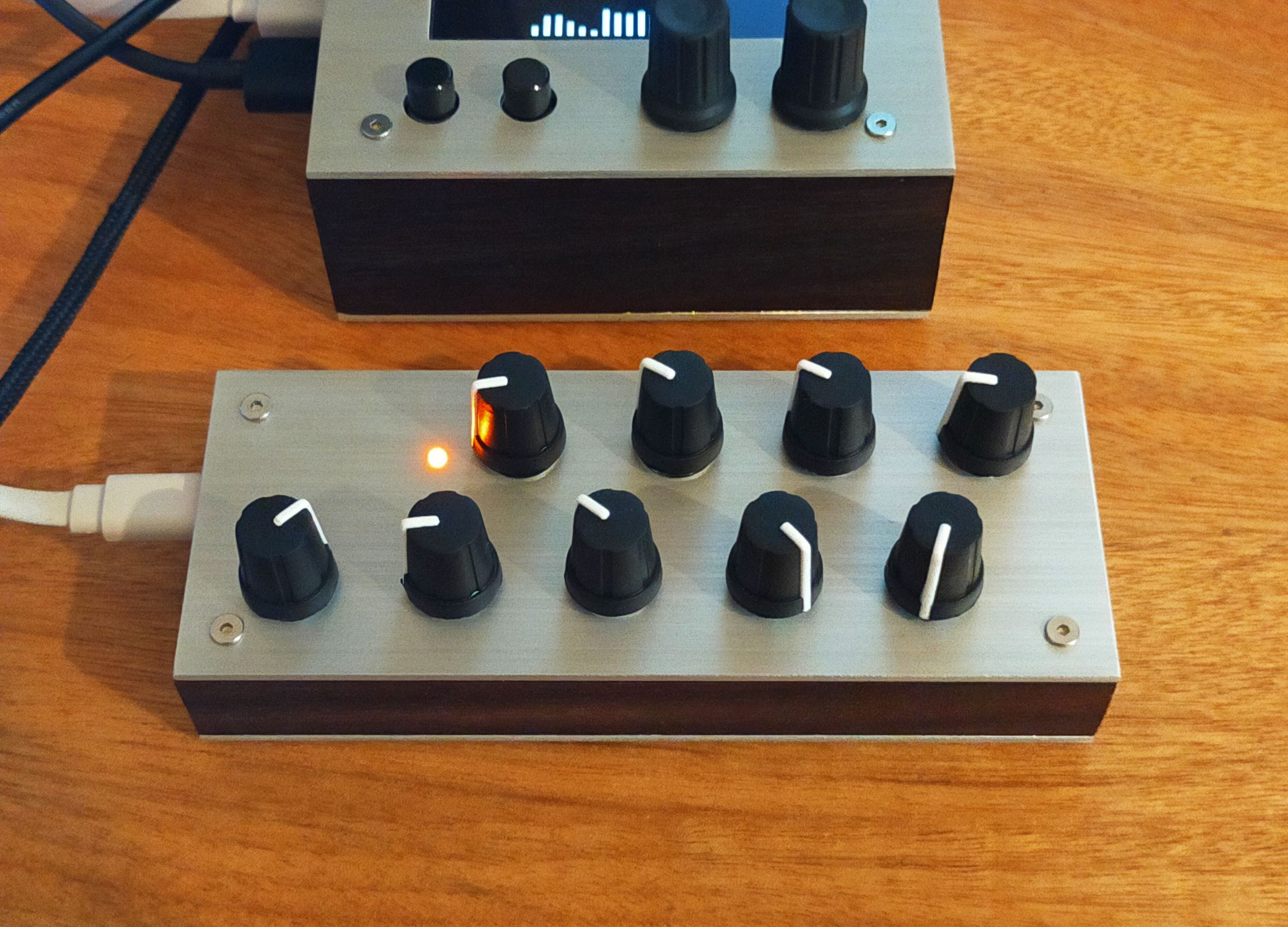 Bleached++ in operation
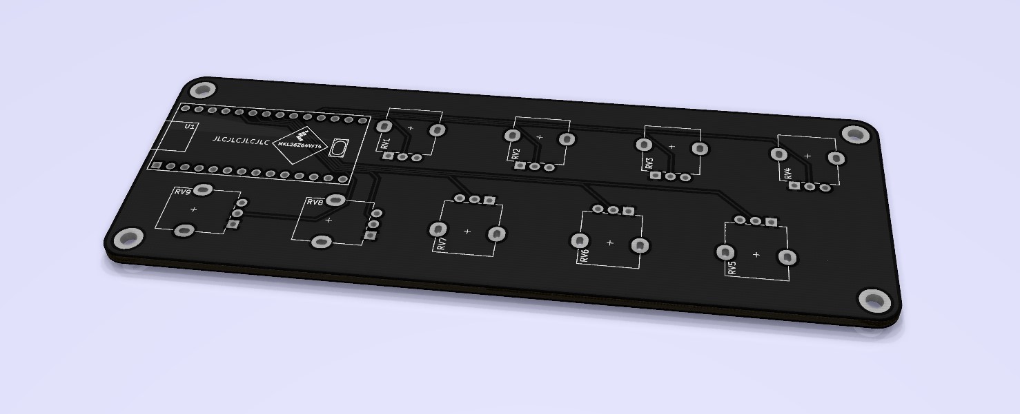 Render of the board
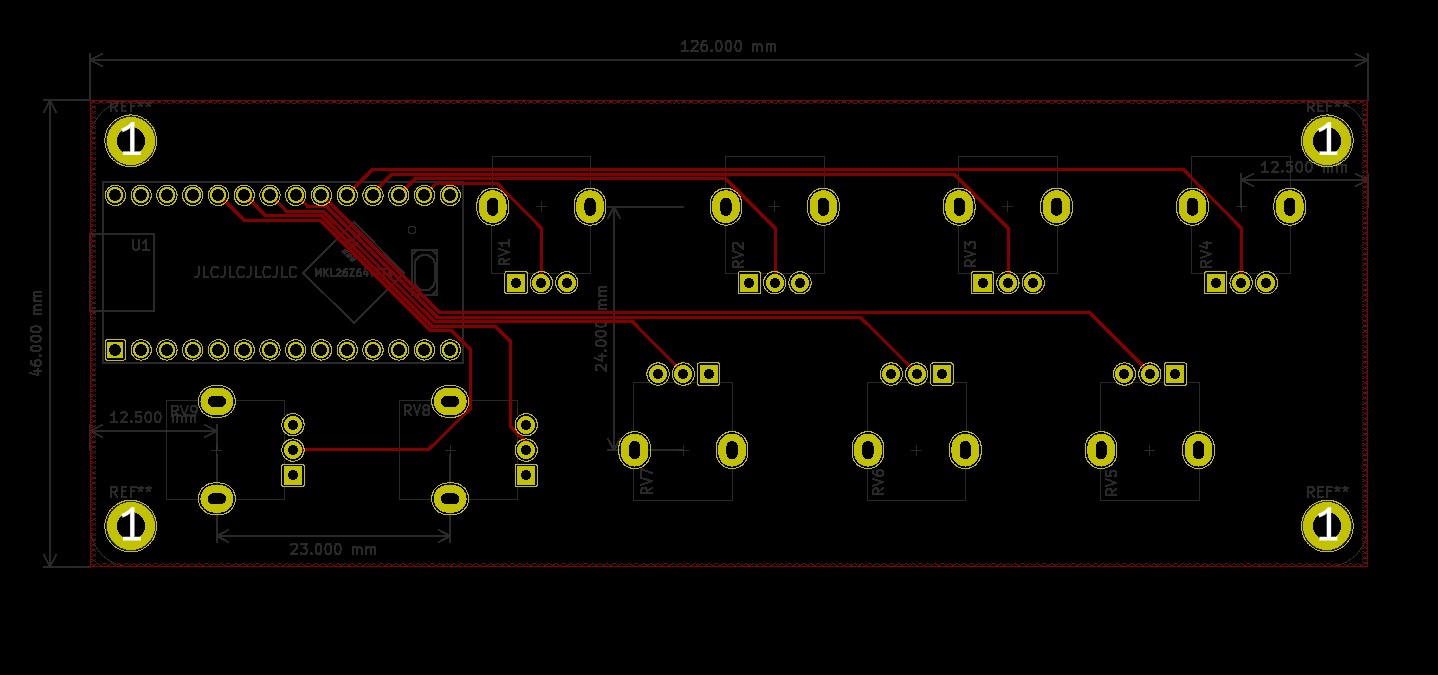 PCB layout with dimensions
1x TeensyLC
2x 14-pin pin headers.
9x 10K linear potentiometers
4x 10mm M2.5 female-female standoffs - to be used between the board and the top panel
4x 5mm* M2.5 male-female standoffs - to be used between the board and the bottom panel (*any length >3mm would be fine)
8x M2.5 5mm length screws
Gerbers are available as a .zip file in the GBR directory. Simply provide the .zip file to a fabrication house. JLCPCB is perhaps the most inexpensive. If using JLCPCB, be sure to use the "specify a location" option to place the unsightly order code under the Teensy, as seen in the render. The option looks like this:

Firmware has been modified from the original Bleached firmware to include the two additional potentiometers.
Also, an additional dual-bank firmware is available incorporating the changes made by mat which allows for a dual 8-bank configuration. The active bank is selectable with the lower-left potentiometer, with feedback provided by the Teensy LED.
An SVG file is provided for making your own top/bottom panels. Use Inkscape or other SVG-reading software to view the file. All elements are seperated into individual layers, so you are able to hide/show the appropriate information. In my case, I make only the outline and all the centrepunch marking crosses visible, then save as a PDF and print at a 1:1 size. I use this as a template for cutting and drilling a blank top panel. I then hide the marking crosses for the LED and potentiometers, repeat the PDF process and use the resultant template for the bottom panel.
Design has been tested as of 16th Sept 2021 and works as intended with the firmware.
| Qty | Value | Footprint | References |
|---|---|---|---|
| 9 | R_POT | Potentiometer_THT:Potentiometer_Alpha_RD901F-40-00D_Single_Vertical | RV1, RV2, RV3, RV4, RV5, RV6, RV7, RV8, RV9 |
| 4 | MountingHole | MountingHole:MountingHole_2.7mm_M2.5_DIN965_Pad | H1, H2, H3, H4 |
| 1 | Teensy-LC_minimal | teensy:Teensy_LC_minimal | U1 |
It measures 126 × 46 mm and has 2 copper layers, 1.6 mm thick.
14 parts. The full list of its parts is on this page, with links to each part's symbol and footprint where PCBKit's library has them.
From the ramphands/bleachedplusplus repository on GitHub, at the commit this page was made from: the board is bleached ++ kicad files/bleachedplusplus.kicad_pcb. PCBKit opens the board in the browser, with nothing to install.
Its repository publishes it under the GPL-3.0 licence: you may reuse it on that licence's terms (keep the author's notice, and for a copyleft licence share your changes alike).
google/mozc-devices
Circuit diagrams and firmware source code for Gboard DIY keyboards


hackclub/OnBoard
💡 Join 1,000 teenagers and make your first PCB with a $100 grant!


Twotoz/C5VRX
Ultra-minimal, zero-CPU 5.8 GHz analog FPV video receiver using ESP32-C5 Wi-Fi 6 PHY MODEM_DIAG, BitScrambler WBFM demodulation & resistor DAC CVBS

