
2 layers158.8 × 172.1 mm
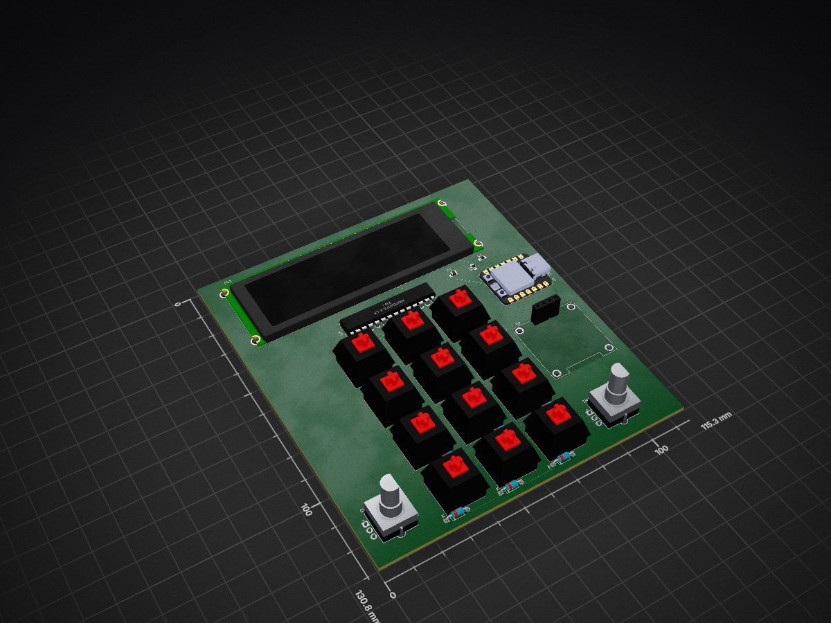
The three Hackpad.kicad files in this directory are the authoritative revision-one KiCad project. They were migrated unchanged from Moksh's active project on 2026-07-18.
Hackpad is an open-source printed circuit board by quantumcompiler32, from the quantumcompiler32/Blip_hackpad repository on GitHub, published under the MIT licence. It is a 2-layer board of 115.3 × 130.8 mm with 33 parts on 46 nets, routed with 303 tracks and 28 vias.
It is built around the NHD-0420CW-AB3. Its parts include 14 switches, 12 diodes, 3 ICs, 2 resistors and 1 capacitor. It belongs with the ESP32 boards of this library.
The three Hackpad.kicad_* files in this directory are the authoritative revision-one KiCad project. They were migrated unchanged from Moksh's active project on 2026-07-18.
Do not commit KiCad locks, automatic backups, local preferences, history folders, cached footprint data, or the unrelated Starter project. Hardware corrections must be made to these sources and documented in the Hardware Change Guide.
Run sh scripts/verify-hardware-source-of-truth.sh to verify the durable source policy. The migration hashes are historical evidence in the baseline findings; they are intentionally not enforced after approved PCB edits. A passing source-policy check does not mean the Hardware Validation Gate has passed.
| Qty | Value | Footprint | References |
|---|---|---|---|
| 12 | 1N4148 | Diode_THT:D_DO-35_SOD27_P7.62mm_Horizontal | D1, D2, D3, D4, D5, D6, D7, D8, D9, D10, D11, D12 |
| 12 | ~ | Button_Switch_Keyboard:SW_Cherry_MX_1.00u_PCB | SW1, SW2, SW3, SW4, SW5, SW6, SW7, SW8, SW9, SW10, SW11, SW12 |
| 2 | 4.7k | Resistor_SMD:R_0805_2012Metric_Pad1.20x1.40mm_HandSolder | R1, R2 |
| 2 | RotaryEncoder_Switch | Rotary_Encoder:RotaryEncoder_Alps_EC11E-Switch_Vertical_H20mm_CircularMountingHoles | SW13, SW14 |
| 1 | 100nF | Capacitor_SMD:C_0805_2012Metric_Pad1.18x1.45mm_HandSolder | C1 |
| 1 | DM-OLED096-636 | DM-OLED096-636:MODULE_DM-OLED096-636 | U2 |
| 1 | MCP23017x-x-SP | Package_DIP:DIP-28_W7.62mm | U3 |
| 1 | NHD-0420CW-AB3 | NHD-0420CW-AB3:LCD_NHD-0420CW-AB3 | DS1 |
| 1 | Seeed Studio XIAO ESP32-S3 | Blip:XIAO_ESP32S3_Socket | U1 |
It measures 115.3 × 130.8 mm and has 2 copper layers, 1.6 mm thick.
33 parts, built around the NHD-0420CW-AB3. The full list of its parts is on this page, with links to each part's symbol and footprint where PCBKit's library has them.
From the quantumcompiler32/Blip_hackpad repository on GitHub, at the commit this page was made from: the board is PCB/Hackpad.kicad_pcb and its schematic PCB/Hackpad.kicad_sch. PCBKit opens the board in the browser, with nothing to install.
Its repository publishes it under the MIT licence: you may reuse it on that licence's terms (keep the author's notice, and for a copyleft licence share your changes alike).

Hypernova-Oy/emb-toveri
Weatherproof embedded user authenticator and authorizator device

hoglet67/RGBtoHDMI
Bare-metal Raspberry Pi project that provides pixel-perfect sampling of Retro Computer RGB/YUV video and conversion to HDMI

mntmn/amiga2000-gfxcard
MNT VA2000, an Open Source Amiga 2/3/4000 Graphics Card (Zorro II/III), written in Verilog

hackclub/OnBoard
💡 Join 1,000 teenagers and make your first PCB with a $100 grant!

Arrow-air/project-quiver
Project Quiver documentation, designs, and project artifacts.

ozel/DIY_particle_detector
A mobile low-cost spectrometer for measuring radioactivity and the energy of ionising radiation like alpha particles and electrons

BlueAndi/Pixelix
Full RGB LED matrix, based on an ESP32 and WS2812B LEDs or emulated LEDs on TFT.